
Semi-conductor device, shallow groove isolation construction forming method

A technology of isolation structure and shallow trench, which is applied in semiconductor devices, semiconductor/solid-state device manufacturing, electric solid-state devices, etc. Trench leakage current, effect of size reduction

Active Publication Date: 2010-12-08
BRIGATES MICROELECTRONICS KUNSHAN
View PDF0 Cites 0 Cited by
  • Summary
  • Abstract
  • Description
  • Claims
  • Application Information

AI Technical Summary

Problems solved by technology

[0007] The technical problem solved by the present invention is that the existing CMOS image sensor technology is prone to leakage current when forming shallow trench isolation, and reduces the dynamic range of the sensor and the maximum signal-to-noise ratio

Method used


Image

  • Semi-conductor device, shallow groove isolation construction forming method
  • Semi-conductor device, shallow groove isolation construction forming method
  • Semi-conductor device, shallow groove isolation construction forming method

Examples


Embodiment Construction

[0034] In traditional CMOS circuits, the width and depth of the isolated shallow trench isolation (STI) determine whether the isolation is effective, and too small a size may cause the STI to break down and fail when subjected to high voltage. Therefore, in the common CMOS device area, STI must ensure sufficient width and depth. But in the pixel unit circuit of CMOS image sensor, such as figure 2 As shown, in order to maintain high photosensitive sensitivity, the potential of the N region of the left photodiode 1 should not be too high, generally not exceeding 0.7V. Therefore, for the pixel unit circuit, the depth and width requirements of the STI are very low, and reducing the size of the STI is equivalent to expanding the P well covering the STI, and can also achieve the purpose of preventing STI leakage current.

[0035] Therefore, in the implementation manner of the present invention, semiconductor devices with different STI sizes can be formed by taking advantage of the...


PUM


Abstract

The invention provides methods for manufacturing semiconductor devices and shallow trench isolation structures. The semiconductor device comprises a semiconductor substrate, device regions formed on the semiconductor substrate and shallow trench isolations formed among devices in each device region, wherein the shallow trench isolations in different device regions are different in size. When the methods are utilized to manufacture a CMOS image sensor, by controlling the opening width of a mask, the etching angle is maintained, the size of the shallow trench isolation in a pixel circuit regionis reduced, thereby effectively preventing forming leakage current of the shallow trench without affecting isolation performance, simultaneously, avoiding influencing the dynamic range of the CMOS image sensor because the area of an N region of a photoelectric diode is reduced.

Description

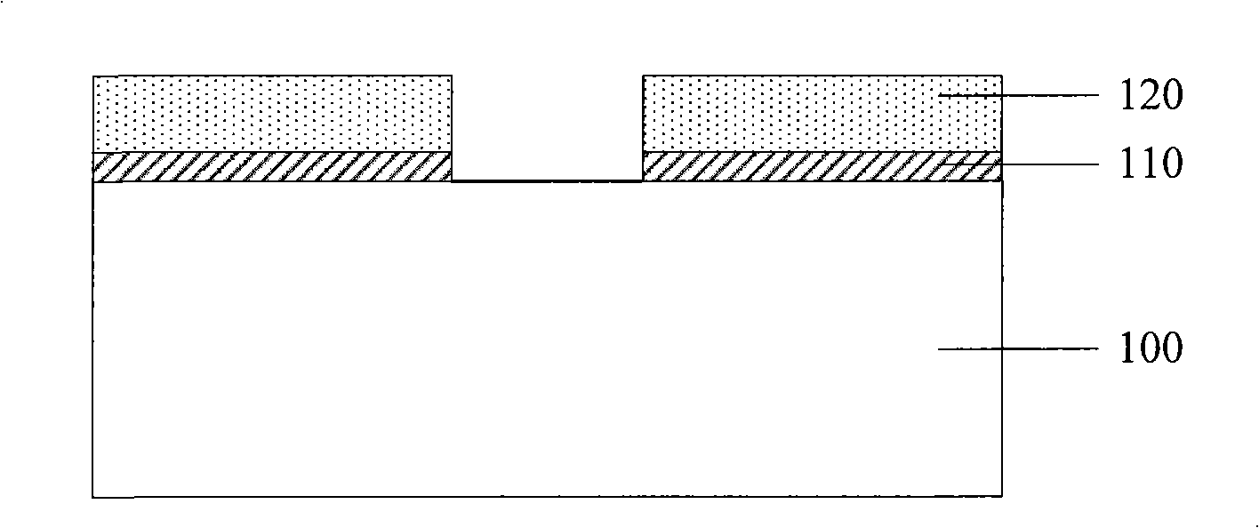
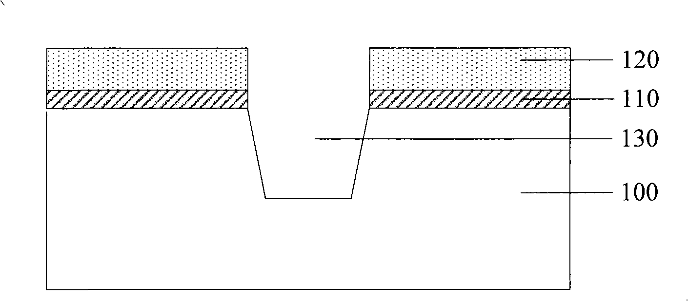
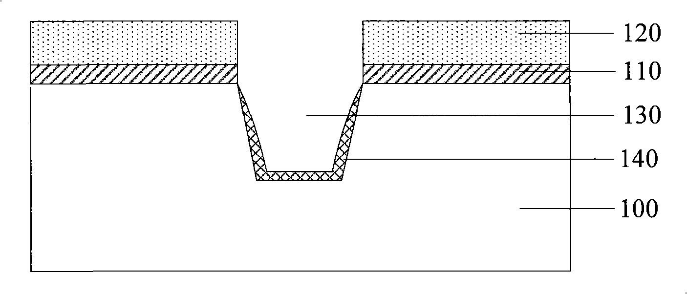
technical field [0001] The present application relates to the field of CMOS process manufacturing, in particular to a method for forming a semiconductor device and a shallow trench isolation structure. Background technique [0002] As semiconductor technology enters the deep sub-micron era, devices below 0.18um technology, such as active region isolation layers of MOS circuits, are mostly manufactured by shallow trench isolation (STI) isolation technology. This process effectively solves the "bird's beak" problem caused by local oxidation isolation in MOS circuits. [0003] refer to Figures 1a to 1f Shown is a typical manufacturing process of the shallow trench isolation structure. First, if Figure 1a , forming a pad oxide layer 110 and an etch stop layer 120 on the semiconductor substrate 100, forming a patterned photoresist on the etch stop layer 120, and using the patterned photoresist as a mask, etching the pad oxide layer 110 and the etch stop layer 120 Corrosion b...

Claims


Application Information

Patent Timeline
Patent Type & Authority Patents(China)
IPC IPC(8): H01L21/762H01L21/308H01L21/3065H01L27/04H01L27/146
Inventor 周谨
Owner BRIGATES MICROELECTRONICS KUNSHAN
Learn More