Bonding material, electronic component, bonding structure and electronic device

A technology for bonding materials and electronic components, applied in welding equipment, welding/cutting media/materials, and assembling printed circuits with electrical components, etc., can solve problems such as inability to obtain bismuth alloys, and achieve the effect of suppressing poor quality and low price

Inactive Publication Date: 2009-06-10
PANASONIC CORP
View PDF1 Cites 2 Cited by
  • Summary
  • Abstract
  • Description
  • Claims
  • Application Information

AI Technical Summary

Problems solved by technology

However, the melting temperature of the eutectic alloy (Bi-4%Zn) composed of 96% by weight of Bi and 4% by weight of Zn is 255°C, and the melting temperature of the eutectic alloy composed of 58% by weight of Bi and 42% by weight of Sn (Bi-42%Sn) has a melting temperature of 138°C, and a eutectic alloy (Bi-65%In) consisting of 35% by weight of Bi and 65% by weight of In has a melting temperature of 72°C. Bismuth alloys with melting temperature above ℃

Method used


Image

  • Bonding material, electronic component, bonding structure and electronic device
  • Bonding material, electronic component, bonding structure and electronic device
  • Bonding material, electronic component, bonding structure and electronic device

Examples


Embodiment Construction

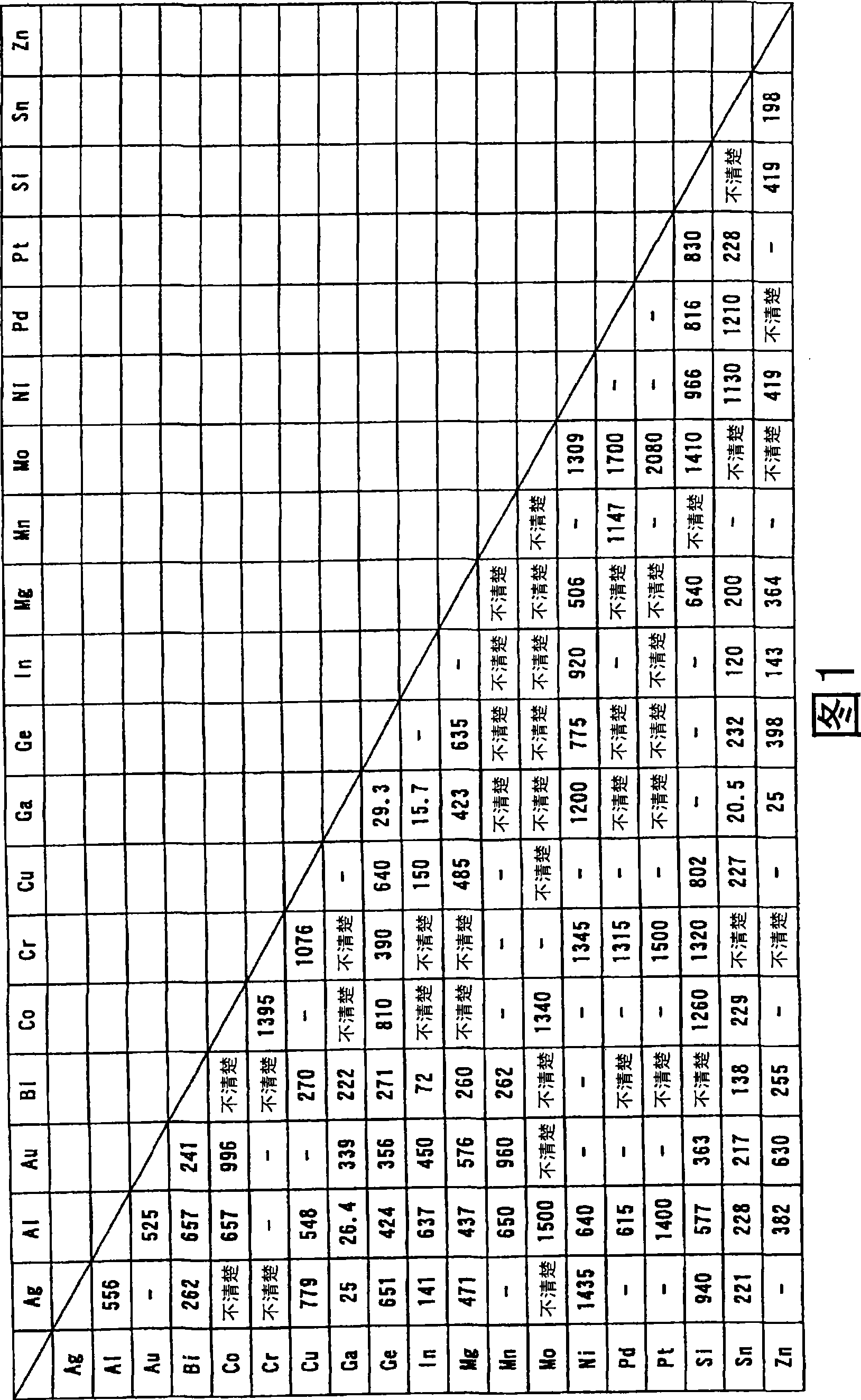
[0047] [joining material]

[0048] The bonding material (1) of the present invention is characterized by containing a bismuth alloy (1) containing Cu and Ge, the balance being Bi, and further containing unavoidable impurities, and containing no lead. In the Bi alloy (1), the Cu content is 0.2 to 0.8 wt%, preferably 0.4 to 0.6 wt%, of the total amount of the bismuth alloy (1). The Ge content is 0.02 to 0.2% by weight of the total amount of the bismuth alloy (1), preferably 0.02 to 0.05% by weight.

[0049] The bonding material (2) of the present invention is characterized by containing a bismuth alloy (2) containing Cu, Ge, and Ni, the remainder being Bi, and further containing unavoidable impurities, and containing no lead.

[0050] In the bismuth alloy (2), the Cu content is 0.2-0.8% by weight of the total amount of the bismuth alloy (2), preferably 0.4-0.6% by weight. The Ge content is 0.02 to 0.2% by weight of the total amount of the bismuth alloy (2), preferably 0.02 to ...


PUM

PropertyMeasurementUnit
melting pointaaaaaaaaaa
particle sizeaaaaaaaaaa

Abstract

A bonding material that has a melting temperature of 270 DEG C or higher and that does not contain lead is inexpensively provided. An electronic element and an electrode of an electronic component are bonded using a bonding material containing an alloy that contains Bi as the main component and that contains 0.2 to 0.8 wt% Cu and 0.02 to 0.2 wt% Ge.

Description

technical field [0001] The present invention relates to a bonding material, an electronic component, a bonding structure, and an electronic device. Background technique [0002] When an electronic component has an electronic element, an electrode, and an electronic element bonding material that joins them, a solder material is generally used as the electronic element bonding material. Electronic components are manufactured by bonding electronic components to electrodes with a solder material. Furthermore, the electronic component is mounted on a substrate such as a mother board using a bonding material different from the electronic element bonding material. For example, a solder material having a melting point of 200 to 230° C. is generally used as a material for joining electronic components such as chip inductors and a mother board. [0003] When the electronic components are mounted on the motherboard, a hot air reflow device is mainly used to heat the electronic compon...

Claims


Application Information

Patent Timeline
Patent Type & Authority Applications(China)
IPC IPC(8): B23K35/26H05K3/34C22C12/00
CPCY02P70/50
Inventor 古泽彰男末次宪一郎坂口茂树中谷公明
Owner PANASONIC CORP
Why Eureka
Try Eureka