Process for preparing p type gallium arsenide ohmic contact

An ohmic contact and gallium arsenide technology, applied in semiconductor devices and other directions, can solve the problem of unsatisfactory p-type gallium arsenide ohmic contact resistance, and achieve the effect of reducing specific contact resistance

Active Publication Date: 2009-06-10
SOI MICRO CO LTD
View PDF0 Cites 5 Cited by
  • Summary
  • Abstract
  • Description
  • Claims
  • Application Information

AI Technical Summary

Problems solved by technology

It can be seen from Table 1 that the current p-type gallium arsenide ohmic contact resistance is not satisfactory

Method used


Image

  • Process for preparing p type gallium arsenide ohmic contact
  • Process for preparing p type gallium arsenide ohmic contact
  • Process for preparing p type gallium arsenide ohmic contact

Examples


Embodiment Construction

[0024] In order to make the object, technical solution and advantages of the present invention clearer, the present invention will be described in further detail below in conjunction with specific embodiments and with reference to the accompanying drawings.

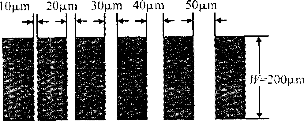
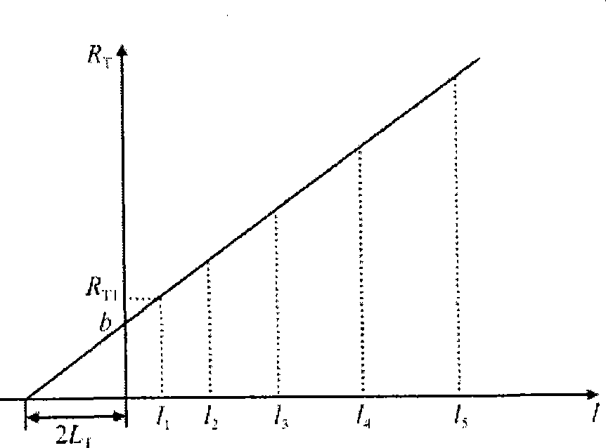
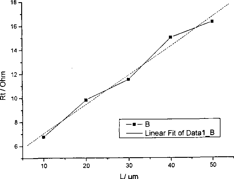
[0025] Since the i-layer itself is non-doped, the resistance of the i-layer is very small due to the conductance modulation effect when the PIN transistor is in forward conduction operation. The forward conduction resistance of GaAs PIN diodes is mainly determined by the bulk resistance of the p- and n-layers and the parasitic ohmic contact resistance. The bulk resistance of the p- and n-layers can be reduced by increasing the doping concentration. The reduction of ohmic contact resistance can be achieved by increasing the surface concentration of gallium arsenide and increasing the contact area between metal and gallium arsenide.

[0026] However, in order to increase the reverse isolation of GaAs PIN diodes, the revers...


PUM

PropertyMeasurementUnit
thicknessaaaaaaaaaa
thicknessaaaaaaaaaa
thicknessaaaaaaaaaa

Abstract

The invention discloses a method for preparing ohmic contact of p-type gallium arsenide. The method comprises: adopting a metal material composition of Pt / Ti / Au as an ohmic contact metal of the p-type gallium arsenide, alloying the metal material composition of Pt / Ti / Au for 1 minute at 375 DEG C, and forming the ohmic contact of the p-type gallium arsenide. The method can effectively reduce specific contact resistivity of the ohmic contact of the p-type gallium arsenide, and reduces the specific contact resistivity of the ohmic contact of the p-type gallium arsenide to be 5.9*10<-6>ohm.cm<2>.

Description

technical field [0001] The invention relates to the technical field of microwave devices, in particular to a method for preparing a p-type gallium arsenide ohmic contact. Background technique [0002] With the advancement of monolithic microwave integrated circuit (MMIC) technology, MMIC circuits are widely used in microwave control circuits, such as antenna switches, phase shifters and attenuators. [0003] Compared with HEMTs, GaAs PIN diodes have the advantages of high cut-off frequency, strong power handling capability, small forward conduction resistance, and small reverse turn-off capacitance. The cut-off frequency is high, so it is widely used in MMIC control circuits. Reducing the forward conduction resistance can effectively reduce the insertion loss of the GaAs PIN diode, and the parasitic ohmic contact resistance will affect the forward conduction resistance, and then affect the MMIC circuit based on the GaAs PIN diode. Therefore, it is very necessary to effecti...

Claims


Application Information

Patent Timeline
Patent Type & Authority Applications(China)
IPC IPC(8): H01L21/28
Inventor 吴茹菲张海英尹军舰
Owner SOI MICRO CO LTD
Why Eureka
Try Eureka