
Non-refrigeration infrared detector array based on polysilicon PN junction and preparing method thereof

An uncooled infrared and detector array technology, applied in the field of infrared detectors, can solve the problems of inconvenience to carry, process incompatibility, and difficulty in miniaturization, and achieve the effects of improving detection sensitivity, avoiding adhesion problems, and reducing heat loss.

Inactive Publication Date: 2009-05-20
INST OF MICROELECTRONICS CHINESE ACAD OF SCI
View PDF0 Cites 18 Cited by
  • Summary
  • Abstract
  • Description
  • Claims
  • Application Information

AI Technical Summary

Problems solved by technology

Photon-type infrared detectors use narrow-bandgap semiconductor materials, such as HgCdTe, InSb, etc., and use the photoelectric effect to realize the conversion of infrared light signals into electrical signals; therefore, they need to work at a temperature of 77K or lower, which requires bulky and complicated Refrigeration equipment, difficult to miniaturize, inconvenient to carry
On the other hand, materials such as HgCdTe and InSb are expensive, difficult to prepare, and incompatible with CMOS processes, so the price of photonic infrared detectors has been high
These have greatly hindered the wide application of infrared cameras, especially in civilian use, there is an urgent need to develop a new type of infrared camera with moderate performance and low price.

Method used


Image

  • Non-refrigeration infrared detector array based on polysilicon PN junction and preparing method thereof
  • Non-refrigeration infrared detector array based on polysilicon PN junction and preparing method thereof
  • Non-refrigeration infrared detector array based on polysilicon PN junction and preparing method thereof

Examples


Embodiment Construction

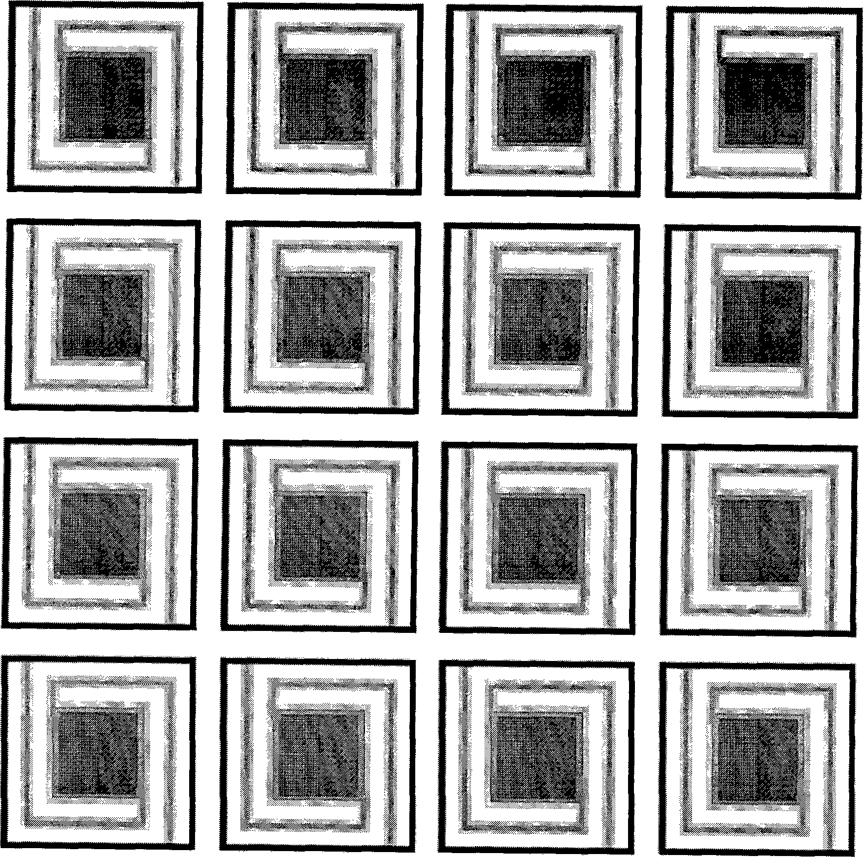
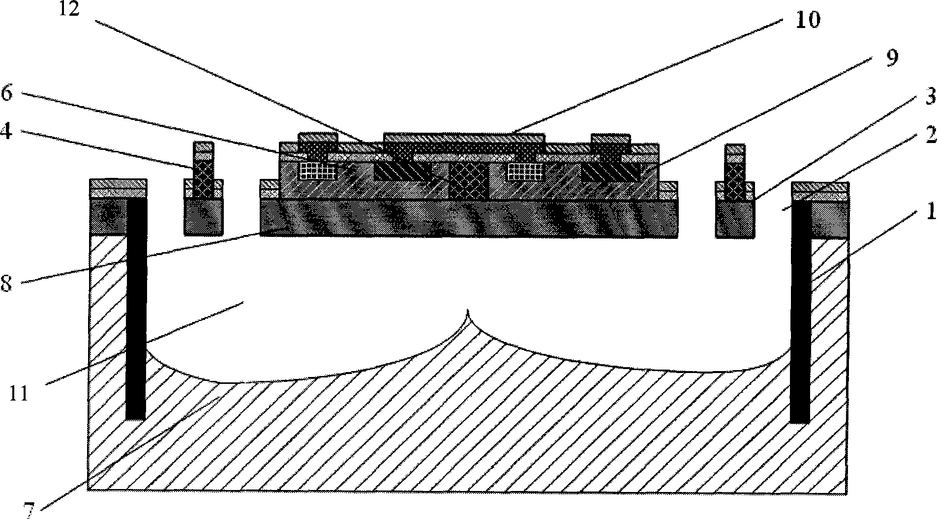
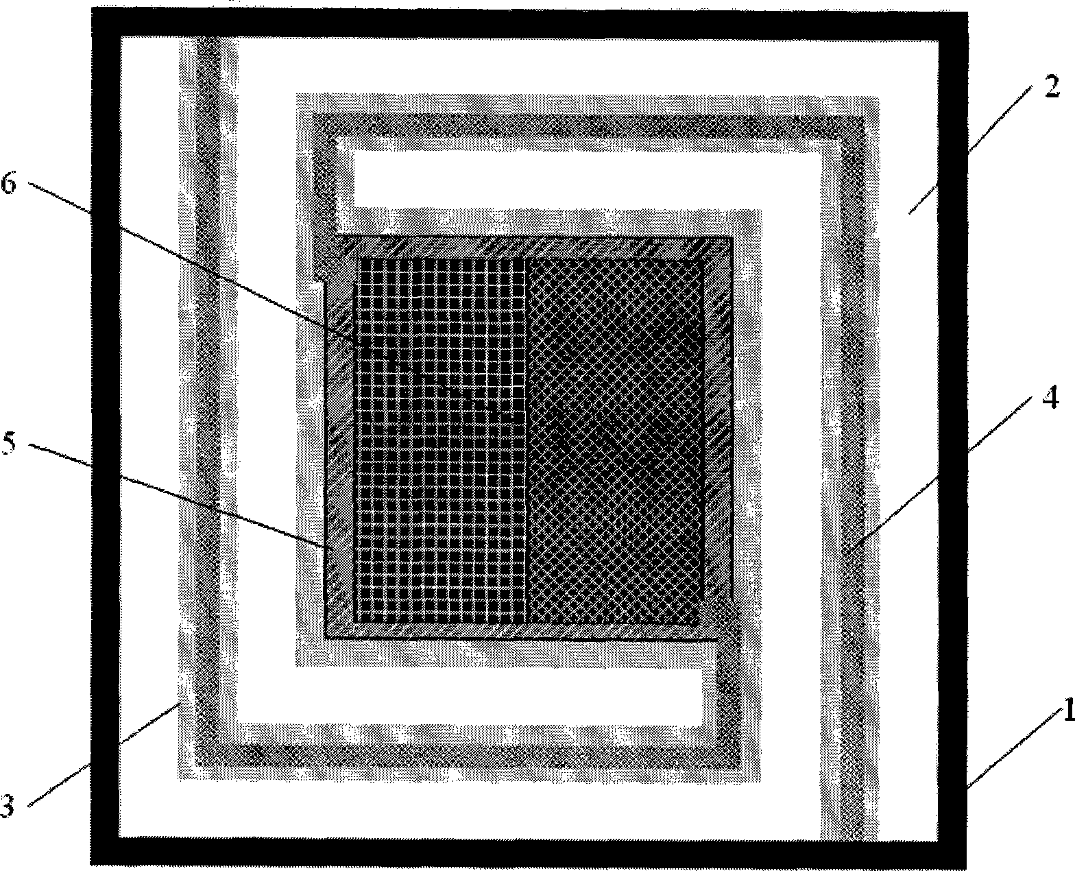
[0027] The invention provides an uncooled infrared detector array based on the polysilicon PN junction temperature characteristics, such as figure 1 As shown, it includes several infrared detection units arranged in sequence. Each of the infrared detection units, such as figure 2 , image 3 As shown, along the longitudinal direction, it includes: a bottom silicon layer 7 , a cavity 11 , a buried oxide layer 8 , and a top silicon layer region 9 above the buried oxide layer 8 .

[0028] The cavity 11 is surrounded by the deep groove 1, the buried oxide layer 8 and the bottom silicon layer 7;

[0029] The deep groove 1 is a lateral barrier layer between the infrared detection unit and other infrared detection units during lateral bottom silicon etching;

[0030] The buried oxide layer 8 is a vertical barrier layer that protects the top silicon layer and the infrared sensitive elements disposed in the top silicon layer from being etched when the bottom silicon is etched vertic...


PUM


Abstract

The invention relates to a non-refrigerated infrared detector array based on temperature characteristics of a polycrystalline silicon PN junction and a preparation method thereof. The preparation method for the array comprises the following steps: step A, etching, filling and flatting a deep groove in order to divide an infrared detection unit transversely; step B, depositing an embedded oxygen layer and a top silicon layer on the front side of a bottom silicon layer; step C, forming an insulated isolation groove on the front side of the top silicon layer in each infrared detection unit and manufacturing a polycrystalline silicon conducting wire on an insulated cantilever beam; step D, setting a plurality of tandem polycrystalline silicon PN junctions on the top silicon layer in each infrared detection unit; step E, forming a double-layer metal wiring; and step F, manufacturing a suspended insulated cantilever beam in the each infrared detection unit, and etching the bottom silicon layer to form a cavity. The preparation method uses favorable temperature characteristics of the polycrystalline silicon PN junction to obtain detection result of infrared radiation strength through measuring changes of voltage at two ends of the polycrystalline silicon PN junction.

Description

technical field [0001] The invention relates to the technical field of infrared detectors, in particular to an uncooled infrared detector based on polysilicon PN junction temperature characteristics and a manufacturing method thereof. Background technique [0002] Infrared imaging technology is widely used in military, industrial, agricultural, medical, forest fire prevention, environmental protection and other fields, and its core component is the Infrared Focal Plane Array (IRFPA). According to the classification of working principle, it can be divided into: photon infrared detector and uncooled infrared detector. Photon-type infrared detectors use narrow-bandgap semiconductor materials, such as HgCdTe, InSb, etc., and use the photoelectric effect to realize the conversion of infrared light signals into electrical signals; therefore, they need to work at a temperature of 77K or lower, which requires bulky and complicated Refrigeration equipment is difficult to miniaturize...

Claims


Application Information

Patent Timeline
IPC IPC(8): G01J5/20
Inventor 何伟明安杰薛惠琼焦斌斌欧毅陈大鹏
Owner INST OF MICROELECTRONICS CHINESE ACAD OF SCI
Learn More