Nano composite electrode preparation for dye sensitization solar cell

A technology for solar cells and dye sensitization, which is applied in the field of preparation of nanocomposite electrodes, can solve the problems of increasing the recombination of photogenerated electrons and holes, increasing the coincidence of photogenerated electrons and holes, and lengthening the electron path, so as to increase the excitation of dyes. The probability of increasing the photoelectric efficiency, the effect of increasing the surface area

Inactive Publication Date: 2011-09-07
PEKING UNIV
View PDF0 Cites 0 Cited by
  • Summary
  • Abstract
  • Description
  • Claims
  • Application Information

AI Technical Summary

Problems solved by technology

However, the network structure electrode formed by sintering nanoparticles also has its problems: there are often a large number of dislocations and defects at the boundary of nanoparticles due to the difference in particle shape and lattice structure, which reduces the mobility of photogenerated electrons in the electrode. , thus greatly increasing the probability of recombination of photogenerated electrons and holes; the network structure formed by the combination of nanoparticles is disordered, which lengthens the path of electrons from excitation to collection to the conductive substrate, thereby also increasing the number of photogenerated electrons and holes. The probability of coincidence causes the loss of photogenerated electrons; the contact between nanocrystalline particles and the conductive substrate is not complete, so that a part of the surface of the conductive substrate is in direct contact with the electrolyte, and the electrons react with the oxidant in the electrolyte, resulting in the loss of photogenerated electrons
However, the actual conversion efficiency of dye-sensitized cells prepared using nanotube arrays as electrodes is still far behind that of traditional nanocrystalline dye cells, mainly due to the relatively small loss in specific surface area of ​​the former’s ordered electrode structure. more, which affects the efficiency of the battery

Method used


Image

  • Nano composite electrode preparation for dye sensitization solar cell
  • Nano composite electrode preparation for dye sensitization solar cell
  • Nano composite electrode preparation for dye sensitization solar cell

Examples


Embodiment Construction

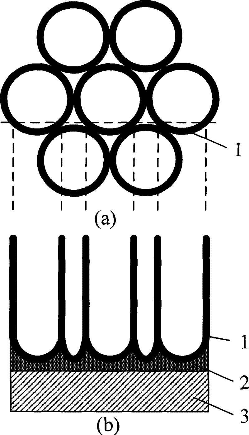
[0019] Below in conjunction with accompanying drawing and specific embodiment the present invention is described in further detail:

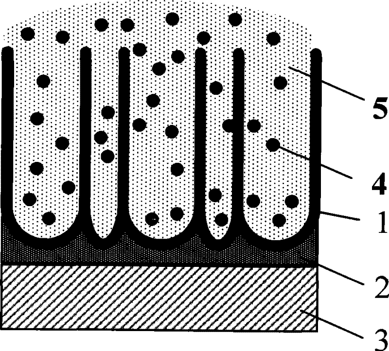
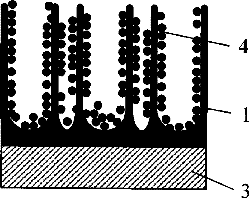
[0020] The transparent conductive substrate adopts the FTO (F-doped tin oxide) conductive glass of Japan Nippon Sheet Glass Company. The conductive glass is cleaned in an ultrasonic water bath and then dried and placed in a magnetron sputtering chamber. The sputtering was carried out in an Ar gas atmosphere, the sputtering power was 1000W, the substrate temperature was room temperature, and the sputtering deposition rate was 10nm / min. Finally, a dense Ti metal film with a thickness of 2um was deposited on the surface of the conductive glass.

[0021] Then the samples were anodized to prepare TiO 2 array of nanotubes. The sample is connected to the positive electrode of the constant voltage source, and the Pt sheet is connected to the negative electrode, and put into the corrosion solution for anodic oxidation operation. The etching solution ...


PUM

PropertyMeasurementUnit
thicknessaaaaaaaaaa

Abstract

The invention discloses a preparation method for a nanometer compound electrode of a dye-sensitized solar cell. The method comprises: using an anodizing method to prepare a TiO2 nanometer tube array on a transparent conductive substrate; then coating a layer of dispersing liquid of TiO2 nanometer particles on the surface of the TiO2 nanometer tube array; finally leading the TiO2 nanometer particles and the TiO2 nanometer tube to be combined by a heating mode and leading the solvent of the dispersing liquid to be volatilized, so as to obtain the semi-conductor compound electrode structure of the dye-sensitized solar cell. As the TiO2 nanometer particles and the TiO2 nanometer tube are combined on the foundation of preparing a sequent nanometer tube array structure, the surface area relative to a single nanometer tube array electrode is increased, thus being capable of absorbing more dyes and improving the photoelectric efficiency of the solar cell. Simultaneously a nanometer particle layer can be used as the diffused reflection layer of the beams transmitting the nanometer tube array, which leads the spreading time of the beams in the tube to be longer and increases the probability of exciting the dyes.

Description

technical field [0001] The invention relates to the dye-sensitized solar cell technology in the field of solar photoelectric utilization, in particular to a preparation method of a nanocomposite electrode of the dye-sensitized solar cell. Background technique [0002] French scientist Henri Becquerel first observed the phenomenon of photoelectric conversion in 1839, but it was not until the advent of the first practical semiconductor solar cell in 1954 that the idea of ​​"converting solar energy into electrical energy" really became a reality. There are many types of solar cells. If the material used is a narrow bandgap semiconductor material with certain absorption in the visible region, this type of solar cell is called a semiconductor solar cell. Since the ability of the wide bandgap semiconductor itself to capture sunlight is very poor, if an appropriate dye is adsorbed on the surface of the semiconductor, with the help of the strong absorption of visible light by the d...

Claims


Application Information

Patent Timeline
Patent Type & Authority Patents(China)
IPC IPC(8): H01M14/00H01G9/20H01G9/04H01L31/18
CPCY02E10/542Y02P70/50
Inventor 康晋锋印海友刘力锋王漪刘晓彦张天舒王旭韩汝琦
Owner PEKING UNIV
Why Eureka
Try Eureka