Ion fluidizing device on chip
A jet device, ion technology, applied in the field of aerospace, can solve the problem of not overcoming high-voltage operation, etc., to achieve the effect of reducing the working voltage, increasing the velocity of the ion jet, and improving the mass flow rate of the ion jet
- Summary
- Abstract
- Description
- Claims
- Application Information
AI Technical Summary
Problems solved by technology
Method used
Image

Examples
Embodiment 1
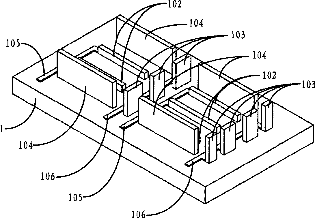
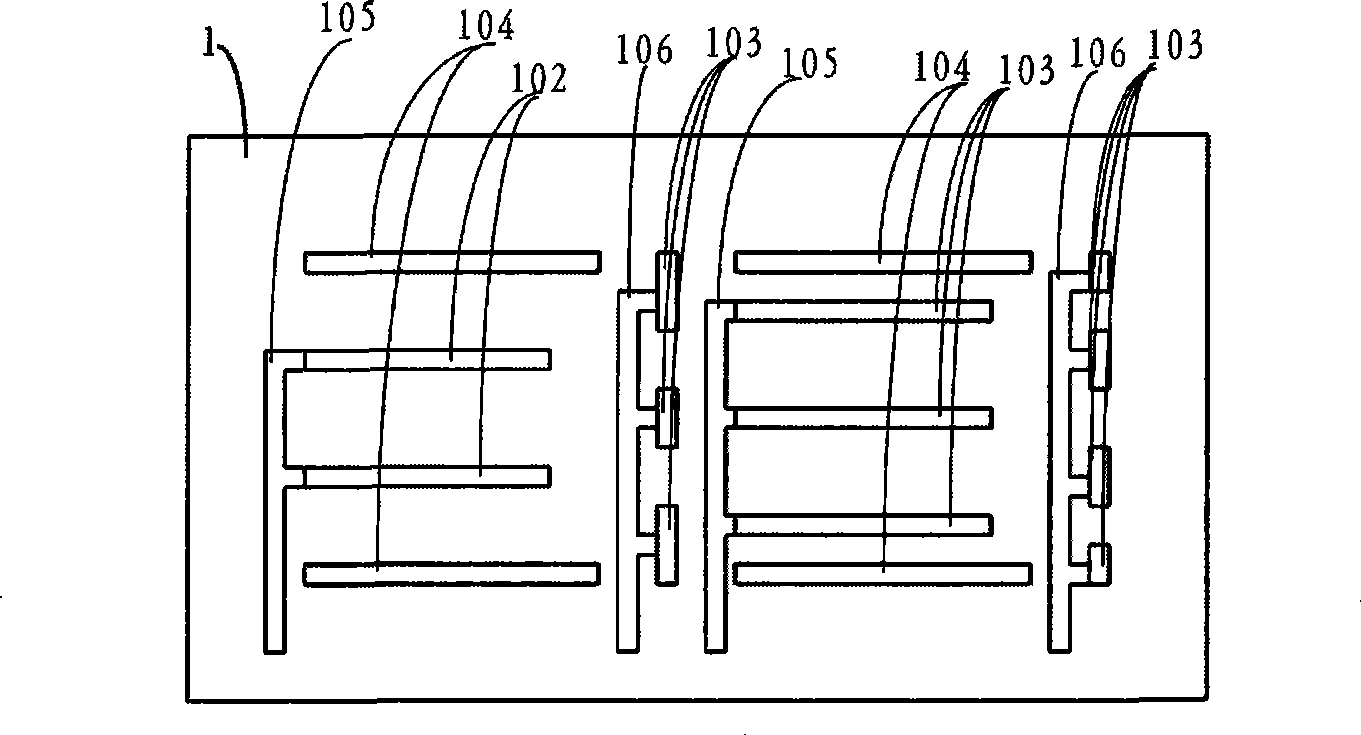
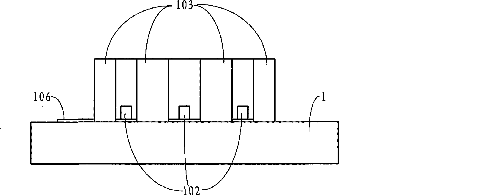
[0034] This embodiment realizes 12 multi-stage on-chip ion jet devices fabricated on flexible substrates, including six single-stage accelerating electrodes, and the structure of every two adjacent single-stage accelerating electrodes is as follows: figure 1 , figure 2 , image 3 Shown.
[0035] The single-stage accelerating electrode is composed of five parts: hollow electrode 103, polarized electrode array 102, flow channel side wall 104, polarized electrode array connection 105, and hollowed-out electrode connection 106. All five parts are arranged on the base on the surface of sheet 1;
[0036] The polarized electrode array 102 is composed of a plurality of discrete planar polarized electrodes whose number is greater than two. Between every two planar polarized electrodes, there is a gas gap to isolate them from each other. The electrode material of each discrete planar polarized electrode , is a conductive or semiconducting electrode material with a large aspect ratio...
Embodiment 2
[0046] This embodiment describes a cooling device using the flow channel sidewall 104 as a cooling fin. A single-stage accelerating electrode constitutes a multi-stage on-chip ion jet device. The electrode structure of any two adjacent accelerating electrodes is as follows: figure 1 , figure 2 , image 3 Shown, specifically described as described in Example 1.
[0047] Wherein, there is a silicon oxide insulating layer with a thickness of about 2 microns on the surface of the substrate 1, which is insulated from all components of the ion jet device on the substrate 1, and a flow channel groove 104 is arranged on the substrate 1, and the width of the groove is 300 μm with a depth of 30 μm. The structure and material arrangement of the polarizing electrode array 102 are the same as those in Embodiment 1. The side wall 104 of the flow channel has a height of 420 μm and a thickness of 50 μm, and is made of single crystal silicon, and its surface is covered with silicon oxide ...
Embodiment 3
[0050] This embodiment describes a cooling device using the sidewall of the channel as a cooling fin, and the difference from Embodiment 2 is that a single-stage on-chip ion jet device is provided.
[0051] A voltage drop of 300V is applied between the polarized electrode array 102 and the hollow electrode 103 of the single-stage fluidic device. By measuring the chip surface temperature, it is found that under the condition that there is a fan as another forced convection source of air, the present invention The solution provided increases the cooling effect of the entire cooling device by about 2 times. Compared with the effect of Example 2, it shows that the ion jet with multi-stage structure is more efficient and can generate greater wind speed and ion mass flow rate, but the single-stage structure is simpler and smaller, and is more suitable for cooling devices In areas where the size of the occupied space is very sensitive.
PUM
| Property | Measurement | Unit |
|---|---|---|
| Height | aaaaa | aaaaa |
| Thickness | aaaaa | aaaaa |
| Thickness | aaaaa | aaaaa |
Abstract
Description
Claims
Application Information
 - R&D
- Intellectual Property
- Life Sciences
- Materials
- Tech Scout
- Unparalleled Data Quality
- Higher Quality Content
- 60% Fewer Hallucinations
Browse by: Latest US Patents, China's latest patents, Technical Efficacy Thesaurus, Application Domain, Technology Topic, Popular Technical Reports.
© 2025 PatSnap. All rights reserved.Legal|Privacy policy|Modern Slavery Act Transparency Statement|Sitemap|About US| Contact US: help@patsnap.com