Wafer reverse side grinding method
A backside grinding and wafer technology, applied in the direction of grinding devices, grinding machine tools, electrical components, etc., can solve the problems of increasing wafer damage rate, high grinding process cost, etc., and achieve the effect of increasing the damage rate
- Summary
- Abstract
- Description
- Claims
- Application Information
AI Technical Summary
Problems solved by technology
Method used
Image

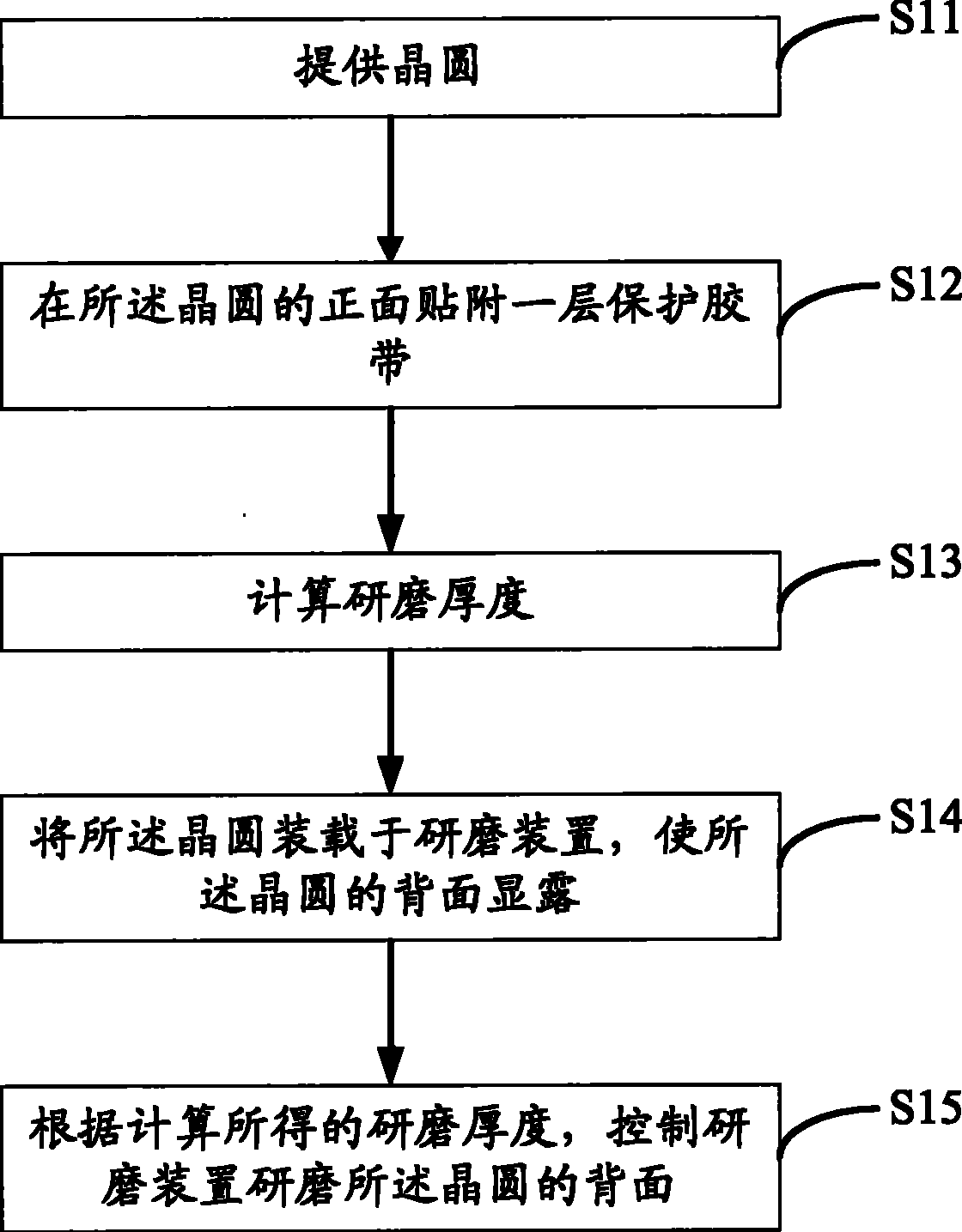

Examples
no. 1 example
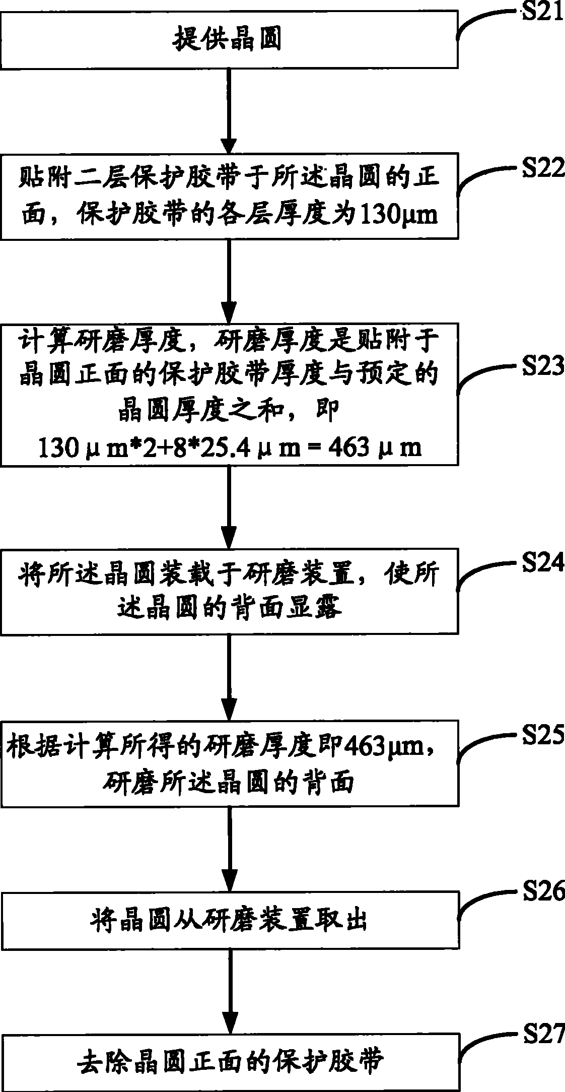
[0039]In this embodiment, the minimum grinding thickness limit of the grinding device is 400 μm, and the thickness of one layer of the protective tape is 130 μm to 160 μm. Taking 130μm as an example, if a layer of protective tape is attached to the front of the wafer, the wafer thickness that the grinding device can achieve is 11mil (130μm+11*25.4μm=410μm>400μm, 130μm+10*25.4μm=384μm 400μm, 130μm*2+5*25.4μm=387μm< 400 μm), that is to say, when a second layer of protective tape is attached to the front of the wafer, the thinnest thickness that the grinding device can grind the wafer to is 6mil. From the above calculation, it can be known that increasing the number of layers of protective tape from one layer to two layers can use the original grinding device to grind the wafer to a wafer thickness that cannot be achieved originally, such as 6 to 10 mil. Therefore, increasing the number of layers of protective tape attached to the front of the wafer can reduce the thinnest thick...
no. 2 example
[0049] The difference between this embodiment and the first embodiment is that the first embodiment does not change the thickness of the protective tape but increases the number of layers of the protective tape to increase the thickness of the protective tape attached to the front of the wafer. The number of layers of protective tape is to choose a thicker protective tape to increase the thickness of the protective tape attached to the front side of the wafer.
[0050] In this embodiment, the steps of grinding the wafer to 8 mil using the above-mentioned grinding device whose minimum grinding thickness limit is 400 μm are as follows: Figure 4 shown.
[0051] Step S41 , providing a wafer, the wafer has a front surface on which integrated circuits are formed and a back surface corresponding to the front surface, and the size of the wafer is 8 inches.
[0052] Step S42, attaching a layer of protective tape to the front surface of the wafer, wherein the thickness of the protecti...
PUM
 Abstract
Description
Claims
Application Information
 - Generate Ideas
- Intellectual Property
- Life Sciences
- Materials
- Tech Scout
- Unparalleled Data Quality
- Higher Quality Content
- 60% Fewer Hallucinations
Browse by: Latest US Patents, China's latest patents, Technical Efficacy Thesaurus, Application Domain, Technology Topic, Popular Technical Reports.
© 2025 PatSnap. All rights reserved.Legal|Privacy policy|Modern Slavery Act Transparency Statement|Sitemap|About US| Contact US: help@patsnap.com