Method for manufacturing gallium nitride compound semiconductor light-emitting device and lamp
A manufacturing method and technology for light-emitting elements, which are applied in semiconductor devices, electrical components, circuits, etc., can solve the problems of increased number of processes, increased manufacturing costs, damage to the surface of gallium nitride compound semiconductors, etc. Effect of small contact resistance
- Summary
- Abstract
- Description
- Claims
- Application Information
AI Technical Summary
Problems solved by technology
Method used
Image
Examples
no. 1 approach
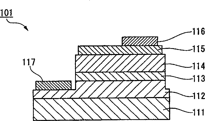
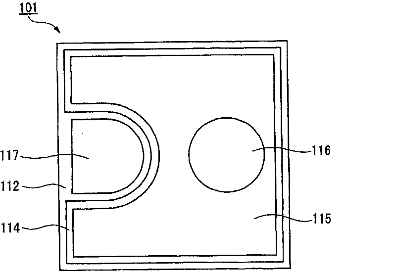
[0101] Hereinafter, regarding the first embodiment of the gallium nitride-based compound semiconductor light-emitting device of the present invention, reference will be made as appropriate. Figure 1~4 while explaining.
[0102] shown in figure 1 The gallium nitride-based compound semiconductor light-emitting element 101 of this embodiment is schematically configured such that an n-type GaN layer 112 , a light-emitting layer 113 , and a p-type GaN layer (p-type semiconductor layer) 114 are formed on a substrate 111 in this order. On the aforementioned p-type GaN layer 114 of the stacked gallium nitride-based compound semiconductor element, a positive electrode 115 formed of a light-transmitting conductive oxide film containing a dopant is stacked, and the p-type GaN layer 114 and the positive electrode (light-transmitting The dopant concentration at the interface of the conductive oxide film 115 is higher than that of the bulk of the translucent conductive oxide film forming ...
experiment example 1
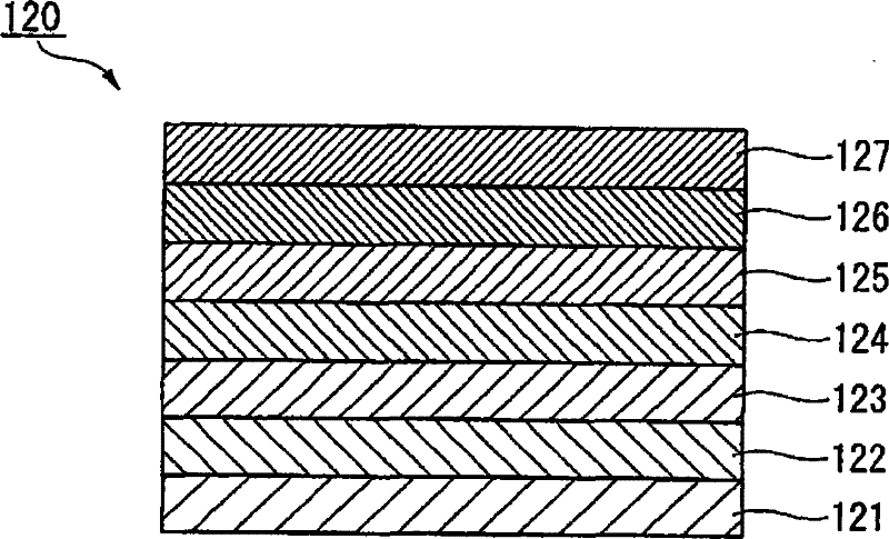
[0144] image 3 , shows a schematic cross-sectional view of an epitaxial structure produced for use in the gallium nitride-based compound semiconductor light-emitting device of this example. and, in figure 1 and figure 2 , shows a schematic cross-sectional view and a schematic plan view of the gallium nitride-based compound semiconductor light-emitting device of the present invention, and will be described below with appropriate reference.
[0145] (Manufacturing of GaN-based compound semiconductor light-emitting devices)
[0146] The multilayer structure of the gallium nitride-based compound semiconductor light-emitting element 120 is composed of a substrate 121 including a c-plane ((0001) crystal plane) of sapphire, with a buffer layer (not shown) including AlN interposed therebetween. Doped GaN base layer (layer thickness=2 μm) 122, Si-doped n-type GaN contact layer (layer thickness=2 μm, carrier concentration=1×10 19 cm -3 ) 123, Si-doped n-type Al 0.07 Ga 0.93 N c...
experiment example 2-5
[0157] Before the formation of the translucent conductive oxide film layer containing ITO, a translucent conductive oxide film contact layer of about 2 nm was formed, and a gallium nitride-based compound semiconductor light-emitting device was produced in the same manner as in Experimental Example 1.
PUM
| Property | Measurement | Unit |
|---|---|---|
| thickness | aaaaa | aaaaa |
| thickness | aaaaa | aaaaa |
| thickness | aaaaa | aaaaa |
Abstract
Description
Claims
Application Information
 - R&D
- Intellectual Property
- Life Sciences
- Materials
- Tech Scout
- Unparalleled Data Quality
- Higher Quality Content
- 60% Fewer Hallucinations
Browse by: Latest US Patents, China's latest patents, Technical Efficacy Thesaurus, Application Domain, Technology Topic, Popular Technical Reports.
© 2025 PatSnap. All rights reserved.Legal|Privacy policy|Modern Slavery Act Transparency Statement|Sitemap|About US| Contact US: help@patsnap.com


