Display
A technology for display devices and protective films, which is applied to lighting devices, light sources, electrical components, etc., can solve the problems of increased manufacturing costs, increased driving electric power, low side wall step coverage, etc., to prevent the appearance of dark spots, good Effect of sealing characteristics and preventing characteristic degradation
- Summary
- Abstract
- Description
- Claims
- Application Information
AI Technical Summary
Problems solved by technology
Method used
Image
Examples
example 1
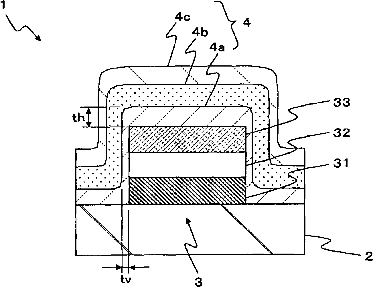
[0073] In Example 1, the formation has figure 2 The configuration shown is the display device 1 . In this example, the high-density silicon nitride film 4a formed under condition 2 of the comparative example, the low-density silicon nitride film 4b formed under condition 3, and the high-density silicon nitride film formed under condition 2 were laminated in the following order. Density of the silicon nitride film 4c to provide the protective film 4. To form protective film 4, silicon nitride films 4a, 4b, and 4c are successively deposited by the plasma CVD method.
[0074] Figure 12 The results of lifetime measurement of the organic electroluminescent device 3 in the display device 1 formed in Example 1 are shown. Figure 12 The lifetimes measured for samples 1 and 4 of the comparative example are also shown.
[0075] Such as Figure 12 As shown, it was confirmed that the display device 1 of Example 1 had a good lifetime which was equivalent to that of the sample 1 usin...
example 2
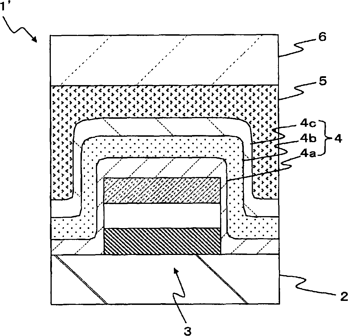
[0081] In Example 2, the formation has image 3 The configuration shown is a display device 1'. In this example, epoxy resin 5 was applied to the entire surface of protective film 4 of the display device formed in Example 1, and a glass substrate (sealing substrate) 6 was bonded with epoxy resin 5 serving as an adhesive.
[0082] The above-formed display device 1' of Example 2 was exposed to a high-temperature and high-humidity environment with a temperature of 80°C and a humidity of 75%. The test results showed that no moisture permeability between the substrate 2 and the glass substrate 6 was observed. The same test results on the display device 1 of Example 1 showed that in a portion of 2 mm or more of silicon nitride (in the protective film 4 ) within the edge of the substrate 2 , moisture-permeable marks were observed. It was thus confirmed that the moisture permeability in the display device can be suppressed by bonding the sealing substrate 6 with the resin 5 .
example 3
[0084] In Example 3, the formation has figure 2 The configuration shown is the display device 1 . In this example, the high-density silicon nitride film 4a formed under condition 2 of the comparative example, the low-density silicon nitride film 4b formed under condition 3, and the silicon nitride film formed under condition 1 were laminated in the following order. A high-density silicon nitride film 4c is used to provide the protective film 4. That is, the films under Condition 2 / Condition 3 / Condition 1 were deposited in order from the lower layer side. In order to form protective film 4, silicon nitride films 4a, 4b, and 4c are successively deposited by the plasma CVD method.
[0085] The display device 1 of Example 3 formed above was exposed to a high-temperature and high-humidity environment with a temperature of 80° C. and a humidity of 75%. The test results showed that the silicon nitride (in the protective film 4 ) within the edge of the substrate 2 ) of 2 mm or mor...
PUM
 Abstract
Description
Claims
Application Information
 - R&D Engineer
- R&D Manager
- IP Professional
- Industry Leading Data Capabilities
- Powerful AI technology
- Patent DNA Extraction
Browse by: Latest US Patents, China's latest patents, Technical Efficacy Thesaurus, Application Domain, Technology Topic, Popular Technical Reports.
© 2024 PatSnap. All rights reserved.Legal|Privacy policy|Modern Slavery Act Transparency Statement|Sitemap|About US| Contact US: help@patsnap.com


