
Patsnap Eureka
For R&D, Patsnap Eureka makes reading and utilizing patents & technical documents easy.
Patsnap Eureka AIR
Designed for self-driven R&D workflows. Generate viable solutions, solve complex R&D challenges, empower your innovation with AI.

Patsnap Eureka Materials
Designed for material experts only. Revolutionize your material R&D, from search, analyze, to developing new materials.

TechResearch
Generate reliable direction feasibility study reports for your R&D in just a few steps.

TechSeek
Discover and master advanced knowledge NOW. Basics, ideas, possibilities, all at once.

TechMind
As an expert in R&D Theories, TechMind can generates customized viable solutions instantly.

TechRisk
Analyze your overall solution with one click, know your potential R&D risks in advance.

TechMonitor
Get weekly tech updates, stay abreast of the latest tech innovations and key insights.
Production method for optical fiber coupling module of glow AlGaInP semiconductor laser
An aluminum gallium indium phosphide and optical fiber coupling technology, which is applied in semiconductor lasers, optical waveguide coupling, lasers, etc., can solve the problems of large beam divergence angle, poor beam quality, and practical application difficulties, and achieve high output fiber laser power, The effect of simple preparation process
- Summary
- Abstract
- Description
- Claims
- Application Information
AI Technical Summary
Problems solved by technology
Method used
Image

Examples
preparation example Construction
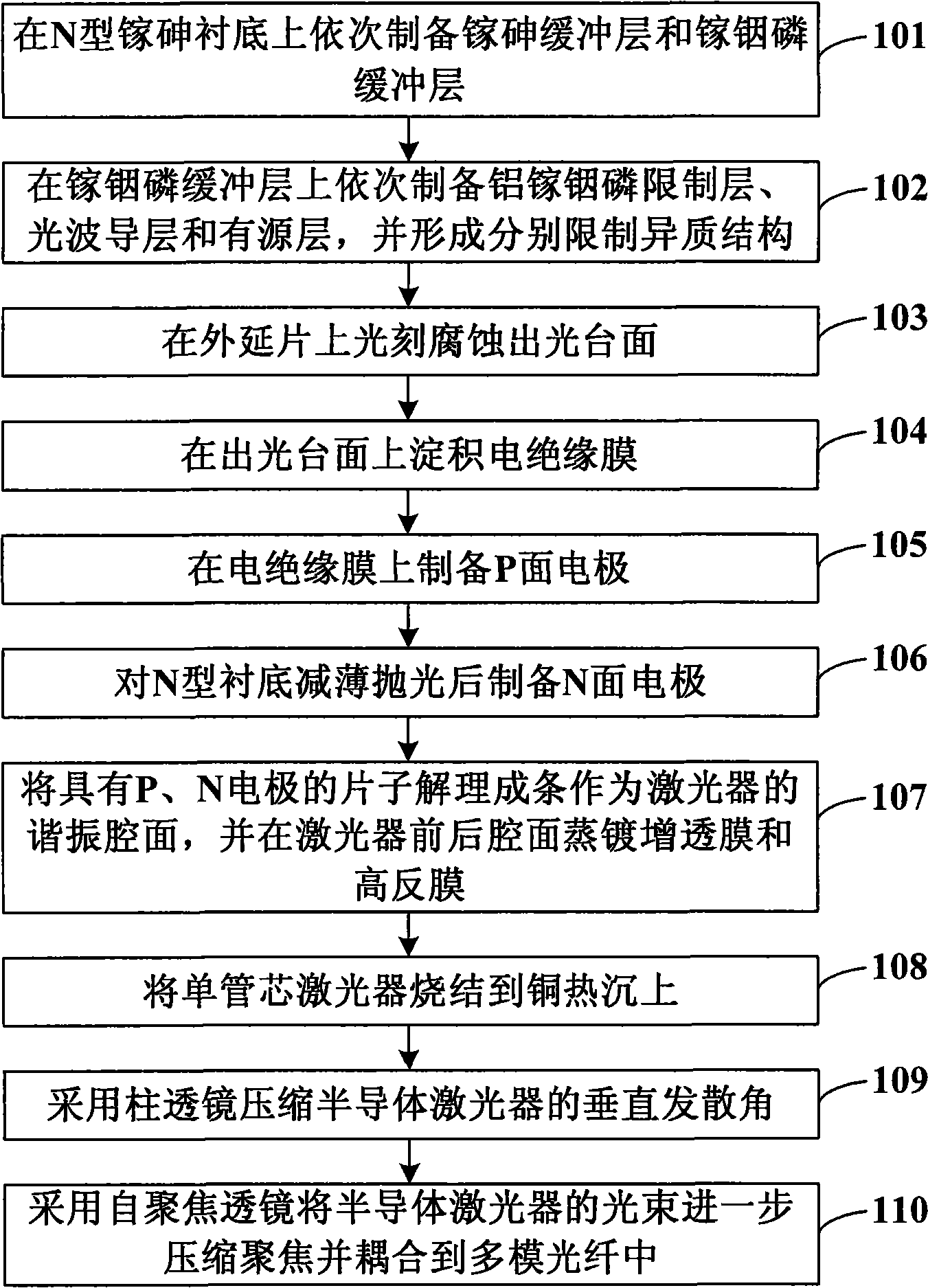
[0043] like figure 1 shown, figure 1 The flow chart of the preparation method of the red light aluminum gallium indium phosphorus semiconductor laser fiber coupling module provided by the present invention, the method includes the following steps:
[0044] Step 101 : sequentially preparing a gallium arsenide buffer layer and a gallium indium phosphorus buffer layer on an N-type gallium arsenide substrate;
[0045] Step 102 : sequentially preparing an AlGaInP confinement layer, an optical waveguide layer and an active layer on the GaInP buffer layer, and forming confinement heterostructures respectively;
[0046] Step 103: photolithography etching the light mesa on the epitaxial wafer;
[0047] Step 104: depositing an electrical insulating film on the light-emitting mesa;
[0048] Step 105: preparing a P-surface electrode on the electrical insulating film;
[0049] Step 106 : preparing an N-surface electrode after thinning and polishing the N-type substrate;
[0050] Step ...
Embodiment
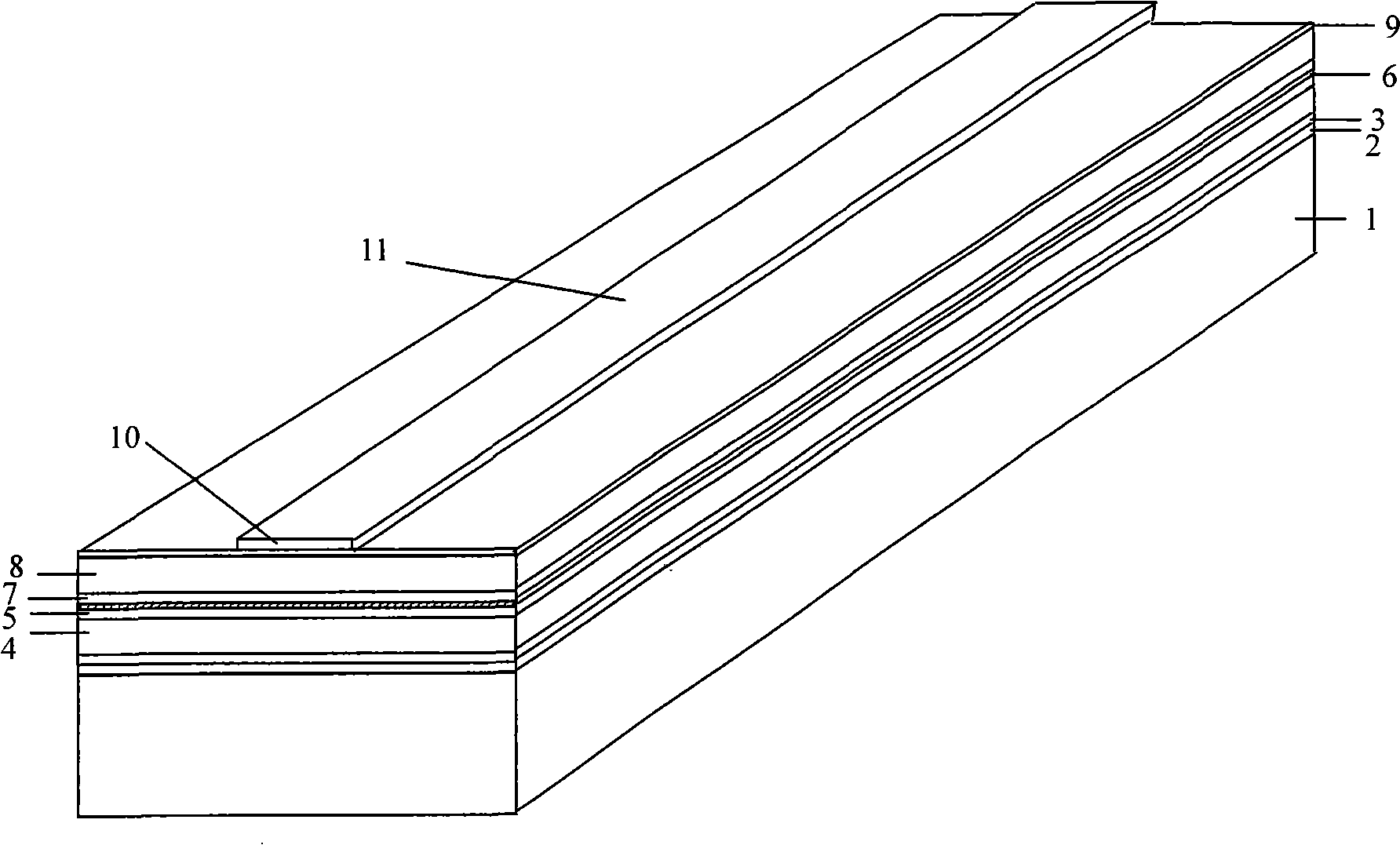
[0068] see figure 2 and image 3 , the preparation method of the red light aluminum gallium indium phosphorus high-power semiconductor laser fiber coupling module provided by the present invention, the specific structure of the device and the preparation process include the following steps:
[0069] (1) An N-type off-angle gallium arsenide substrate 1 is selected, and an N-type gallium arsenide buffer layer 2 and an N-type gallium indium phosphorus buffer layer 3 are epitaxially grown on the N-type gallium arsenide substrate 1 by a metal organic compound vapor deposition method.
[0070] (2) On the N-type Gallium Indium Phosphorus buffer layer 3, epitaxially grow the N-type AlGaInP lower cladding layer 4 with high Al composition, the AlGaInP lower optical waveguide layer 5 with low Al composition, and the active region sequentially 6. Aluminium Gallium Indium Phosphorus upper optical waveguide layer 7 with low Al composition, P-type AlGaInP upper cladding layer 8 with high A...
PUM
| Property | Measurement | Unit |
|---|---|---|
| Thickness | aaaaa | aaaaa |
Abstract
Description
Claims
Application Information
 - R&D Engineer
- R&D Manager
- IP Professional
- Industry Leading Data Capabilities
- Powerful AI technology
- Patent DNA Extraction
Browse by: Latest US Patents, China's latest patents, Technical Efficacy Thesaurus, Application Domain, Technology Topic, Popular Technical Reports.
© 2024 PatSnap. All rights reserved.Legal|Privacy policy|Modern Slavery Act Transparency Statement|Sitemap|About US| Contact US: help@patsnap.com