Process for preparing isolation of shallow channel

A manufacturing method and shallow trench technology, applied in semiconductor/solid-state device manufacturing, electrical components, circuits, etc., can solve problems such as threshold voltage drop, leakage current increase, affecting device performance, etc., to prevent threshold voltage drop, The effect of reducing leakage current

Active Publication Date: 2008-11-26
SEMICON MFG INT (SHANGHAI) CORP +1
View PDF1 Cites 11 Cited by
  • Summary
  • Abstract
  • Description
  • Claims
  • Application Information

AI Technical Summary

Problems solved by technology

[0008] However, when the pad oxide layer 12A is removed by the hydrofluoric acid solution in the manufacturing method of the above shallow trench isolation, the hydrofluoric acid solution will also corrode the oxide layer 22, so that the The top edge forms a groove, such as Image 6 The groove 21 shown in the figure causes the device close to the groove 21 to increase the leakage current and decrease the threshold voltage when the device works in the sub-threshold region, which affects the performance of the device

Method used


Image

  • Process for preparing isolation of shallow channel
  • Process for preparing isolation of shallow channel
  • Process for preparing isolation of shallow channel

Examples


Embodiment Construction

[0034] The specific embodiments of the present invention will be described in detail below in conjunction with the accompanying drawings.

[0035] Figure 7 It is a flow chart of an embodiment of the manufacturing method of the shallow trench isolation of the present invention.

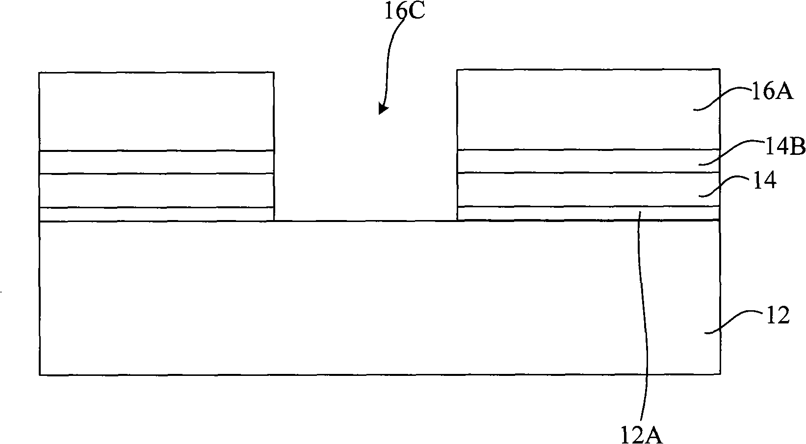
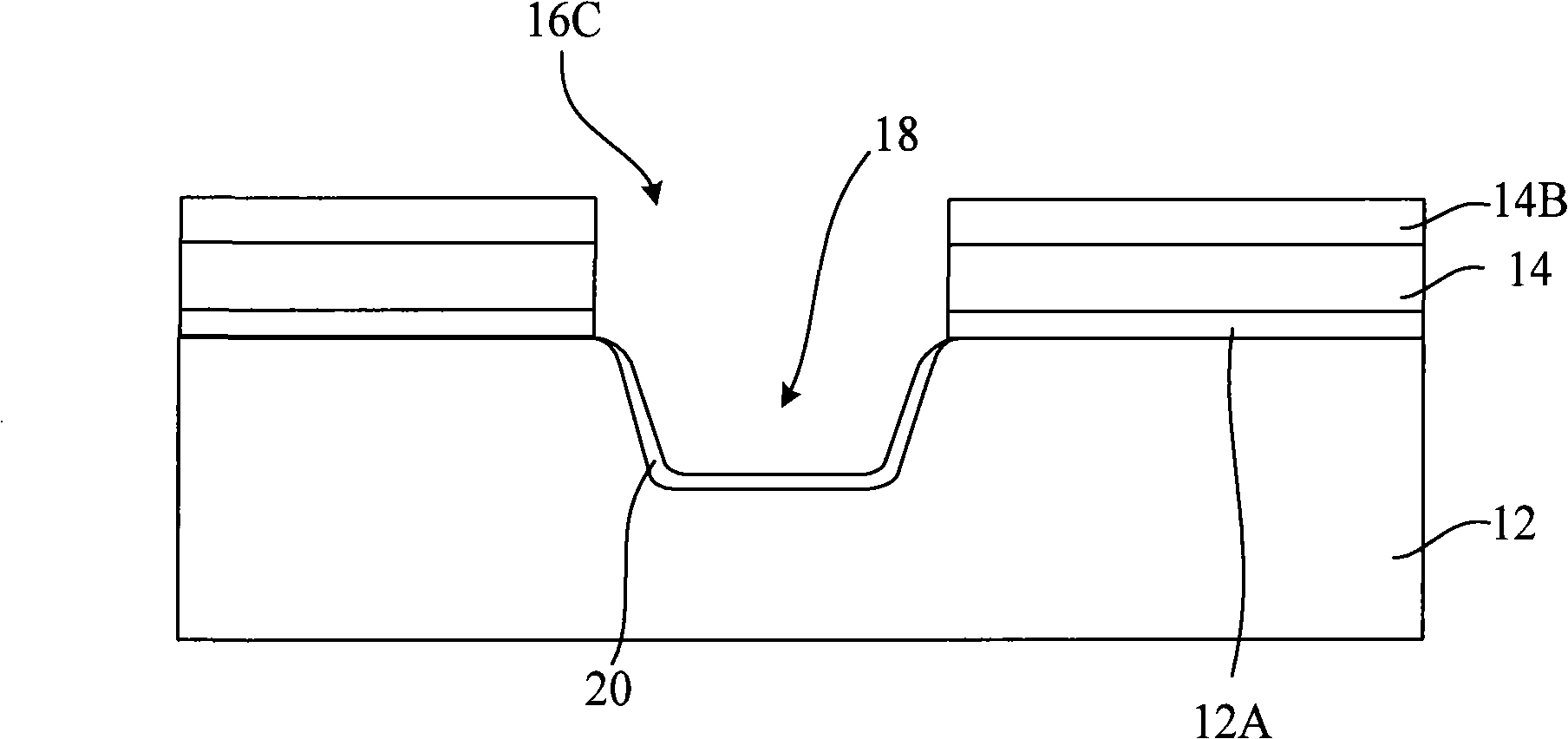
[0036] Such as Figure 7 As shown, in step 1, a semiconductor substrate is provided (S100); a pad oxide layer and a hard mask layer are sequentially formed on the semiconductor substrate, a groove is formed in the semiconductor substrate, and a pad is formed on the pad The oxide layer and the hard mask layer have openings at positions corresponding to the grooves.

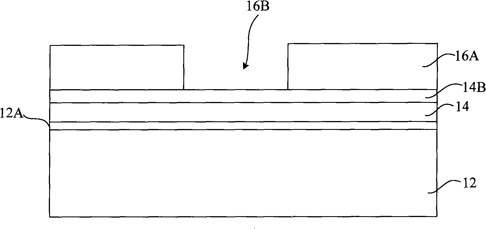
[0037] Such as Figure 8 As shown in the cross-sectional schematic diagram, the semiconductor substrate 100 can be one of single crystal silicon, polycrystalline silicon, and amorphous silicon, and the semiconductor substrate 100 can also be one of silicon-germanium compounds and silicon-gallium compounds. The substrate 100 may include...


PUM


Abstract

A manufacturing method of shallow groove insulation comprises providing a semiconductor substrate, positioning sequentially formed a pad oxide layer and a hard mask layer, forming a groove in the semiconductor substrate, arranging an opening in a position corresponding to the groove in the pad oxide layer and the hard mask layer, forming a medium layer in the groove and on the hard mask layer, removing the medium material on the hard mask layer by planarization technology, etching the medium layer in the groove to reduce the height difference between the medium layer surface and the semiconductor substrate surface, and lead the edge of the medium layer to form a protuberance. The manufacturing method of shallow groove insulation can reduce the depth of the top edge groove of the shallow groove insulation, and improve the element properties.

Description

technical field [0001] The invention relates to the technical field of semiconductor manufacturing, in particular to a method for manufacturing shallow trench isolation (Shallow Trench Isolation, STI). Background technique [0002] With the development of semiconductor manufacturing technology to high-tech nodes, the device-to-device isolation technology in semiconductor integrated circuits has also developed from the original Local Oxidation of Silicon (LOCOS) to shallow trench isolation. Shallow trench isolation is formed by forming a trench on a semiconductor substrate and filling the trench with a dielectric material. The Chinese patent application document with publication number CN 1649122A discloses a manufacturing method of shallow trench isolation. Figure 1 to Figure 5 It is a schematic cross-sectional view of the structure corresponding to each step of the manufacturing method of the shallow trench isolation disclosed in the Chinese patent application document. ...

Claims


Application Information

Patent Timeline
Patent Type & Authority Applications(China)
IPC IPC(8): H01L21/762
Inventor 刘石香
Owner SEMICON MFG INT (SHANGHAI) CORP
Why Eureka
Try Eureka