Composite hard mask layer, metal-oxide-semiconductor transistor and manufacturing method thereof

A technology of oxide semiconductor and hard mask layer, applied in semiconductor/solid-state device manufacturing, semiconductor devices, electrical components, etc., can solve problems such as damage to other components, damage to other components, etc., to resist wear and tear and improve yield. Effect

Active Publication Date: 2011-11-09
UNITED MICROELECTRONICS CORP
View PDF0 Cites 0 Cited by
  • Summary
  • Abstract
  • Description
  • Claims
  • Application Information

AI Technical Summary

Problems solved by technology

[0008] Therefore, the present invention hereby provides a method for manufacturing MOS transistors using a composite hard mask, so as to improve the damage to other components due to consumption of the hard mask layer in the prior art, and damage to other components when the hard mask layer is removed. lack of

Method used


Image

  • Composite hard mask layer, metal-oxide-semiconductor transistor and manufacturing method thereof
  • Composite hard mask layer, metal-oxide-semiconductor transistor and manufacturing method thereof
  • Composite hard mask layer, metal-oxide-semiconductor transistor and manufacturing method thereof

Examples


Embodiment Construction

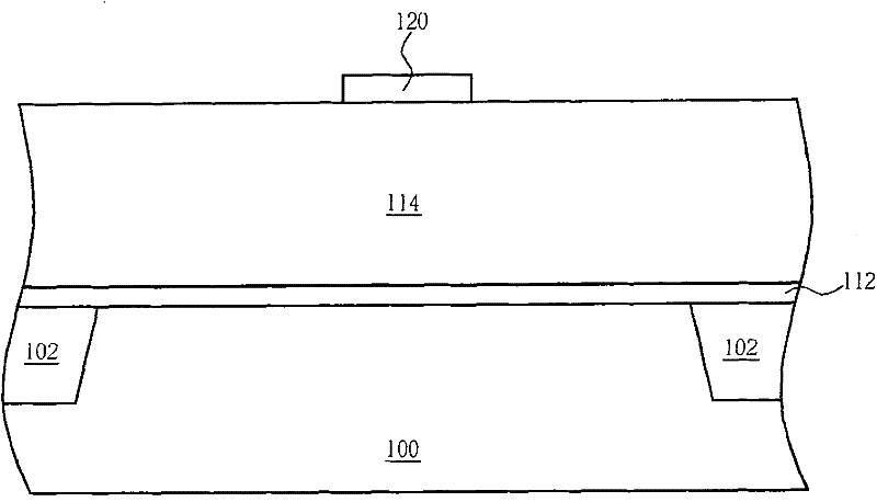
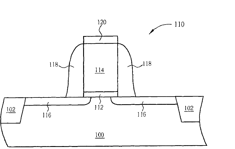
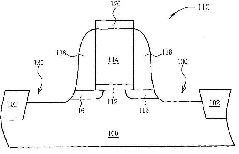
[0037]Please refer to FIG. 5 to FIG. 11 . FIG. 5 to FIG. 11 are the first preferred embodiment of the manufacturing method of the composite hard mask layer provided by the present invention. As shown in FIG. 5 , firstly, a substrate 200 is provided, such as a silicon substrate, on which a plurality of shallow trench isolations (shallow trench isolation, STI) 202 have been formed. Subsequently, a dielectric layer 212 , a polysilicon layer 214 , and a first hard mask layer 220 are sequentially formed on the substrate 200 . The first hard mask layer 220 includes silicon oxide (SiO), silicon nitride (SiN), silicon oxynitride (SiON), silicon carbide nitride (SiCN), silicon carbide (SiC), silicon carbide containing oxygen (SiOC), Silicon-rich-nitride (SRN), high temperature oxide (HTO), anti-reflective bottom layer, or bis (tert-butylamino) silane (Bis (tert-butylamino) silane, BTBAS) . A photoresist layer 222 is formed on the first hard mask layer 220, and the photoresist layer 2...


PUM


Abstract

The invention discloses a method for preparing metal oxide semiconductor transistor by utilizing composite hard mask layer, which includes steps: providing a substrate which surface contains a dielectric layer and a multi-crystal silicon layer; forming a composite hard mask containing a middle hard mask and a side wall hard mask which covers side wall of the middle hard mask on the multi-crystal silicon layer; carrying a first etching technique: etching the multi-crystal silicon layer and the dielectric layer by using the composite hard mask as etching mask, and forming a grid structure; carrying a second etching technique: forming grooves respectively on substrate at two sides of the grid structure; carrying selectivity epitaxial growth technique: forming epitaxial layers respectively inthe grooves. The invention also discloses a composite hard mask layer and a metal oxide semiconductor transistor.

Description

technical field [0001] The present invention relates to a method for manufacturing a metal-oxide semiconductor transistor (MOS transistor) using a composite hard mask layer, especially a method for growing a metal-oxide semiconductor transistor (MOS transistor) using selective epitaxial growth (hereinafter referred to as SEG). Methods of fabricating MOS transistors. Background technique [0002] Selective epitaxial growth (SEG) technology is mainly to form an epitaxial layer with the same lattice arrangement as the substrate on the surface of a single crystal substrate, which is used in the manufacture of many semiconductor devices, such as raised source / drain (raised source / drain) ) transistors have the advantages of good short channel characteristics and low parasitic resistance, and at the same time, through the existence of an increased epitaxial layer, it can avoid the trouble of excessive consumption of silicon substrate when forming metal silicide; while the embedded ...

Claims


Application Information

Patent Timeline
Patent Type & Authority Patents(China)
IPC IPC(8): H01L21/336H01L21/314H01L29/78
Inventor 黄慧玲陈明新李年中陈立勋戴炘
Owner UNITED MICROELECTRONICS CORP
Why Eureka
Try Eureka