Method of filling redundancy for semiconductor manufacturing process and semiconductor device

A technology of filling method and manufacturing process, which is applied in semiconductor/solid-state device manufacturing, semiconductor devices, semiconductor/solid-state device components, etc., can solve problems such as adverse side effects, increase parasitic capacitance, and reduce device performance, so as to reduce power consumption, Reduce the amount of redundant metal, the best effect of redundant layout distribution

Active Publication Date: 2008-07-30
TAIWAN SEMICON MFG CO LTD
View PDF0 Cites 31 Cited by
  • Summary
  • Abstract
  • Description
  • Claims
  • Application Information

AI Technical Summary

Problems solved by technology

These problems will be magnified as new manufacturing process technologies emerge and circuit designs become more complex
In addition, unnecessary redundancy factors may reduce the performance of the device, such as increased parasitic capacitance and other undesirable side effects

Method used


Image

  • Method of filling redundancy for semiconductor manufacturing process and semiconductor device
  • Method of filling redundancy for semiconductor manufacturing process and semiconductor device
  • Method of filling redundancy for semiconductor manufacturing process and semiconductor device

Examples


Embodiment Construction

[0034] In order to make the present invention easier to understand, the following descriptions will be written in the form of embodiments or examples, together with the accompanying drawings. However, these embodiments or examples are not intended to limit the scope of the present invention. Any changes and further modifications will be described in the embodiments, or can be understood by those of ordinary skill in the art based on the content disclosed in the present invention. Furthermore, the presence of one or more adjacent elements does not imply that there are no intervening elements present. Furthermore, reference numerals may appear repeatedly in these embodiments, but it does not mean that the characteristics of one embodiment can be applied to another embodiment, even if they have the same reference numerals.

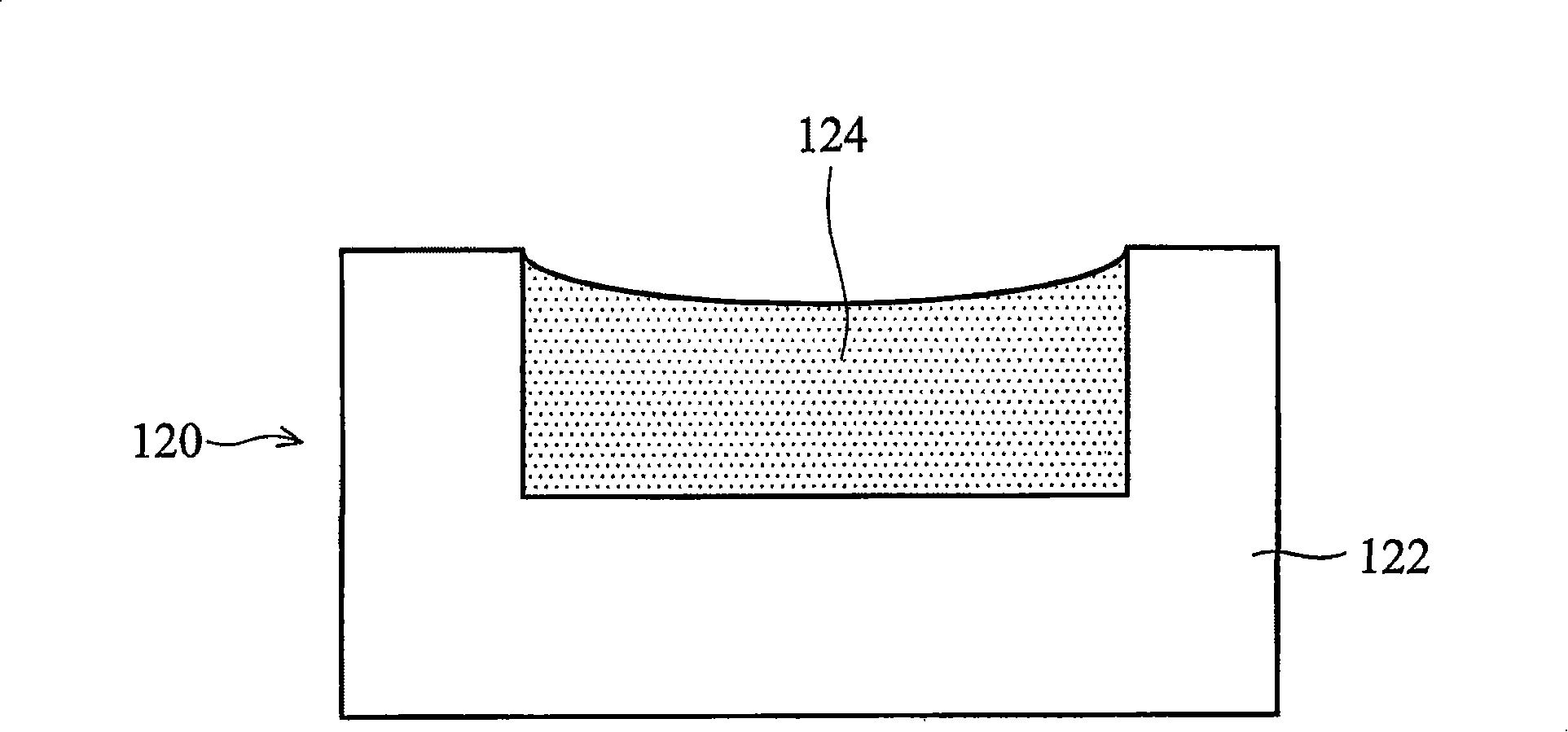
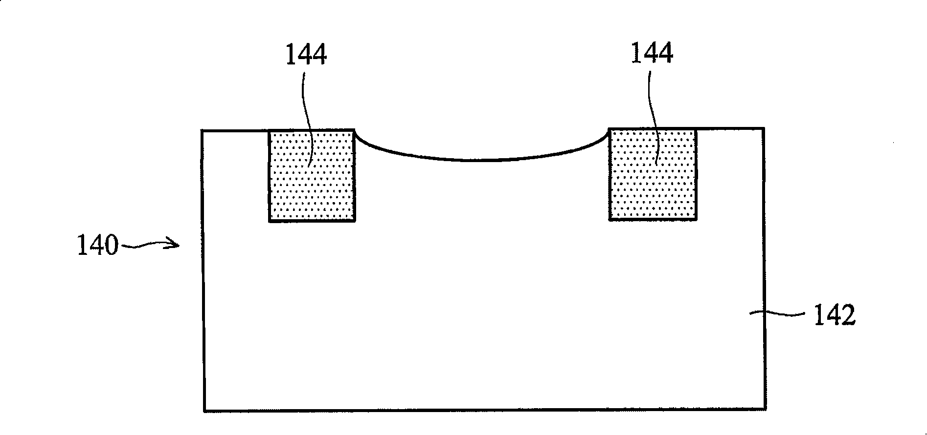
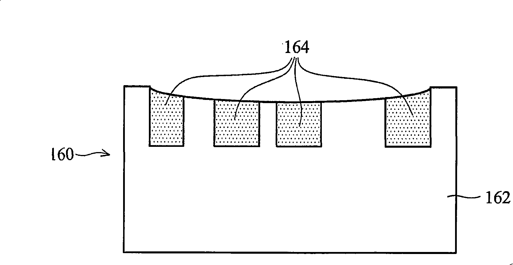
[0035] FIG. 1 is a cross-sectional view 100 of four semiconductor wafers showing dishing and erosion phenomena caused by chemical mechanical polishing. exi...


PUM


Abstract

A dummy filling method for a semiconductor manufacturing process provides a circuit pattern and generates a density report of the circuit pattern to identify a feasible area for dummy insertion. The method also includes using the density report to simulate a planarization manufacturing process and identifying hot spots on the circuit pattern, filling virtual redundant patterns in the feasible area, and then adjusting the density report. The method simulates the planarization process using the adjusted density report until the hot spot is removed. The invention can reduce the amount of redundant metal in circuit design and save photomask time, CPU time, and signal storage memory. This will help design timing closure (time closure) faster and easier.

Description

technical field [0001] The present invention relates to a semiconductor manufacturing process, in particular to a method for ensuring chemical mechanical polishing (CMP) performance with an optimal number of dummy insertions. Background technique [0002] The dual damascene fabrication process is commonly used in semiconductor manufacturing as chip sizes shrink and technology reaches sub-micron. In the dual damascene manufacturing process, copper is generally used as the conductive material for the connection. Other conductive materials include tungsten, titanium, titanium nitride. Correspondingly, silicon oxide, fluorine-doped silicon glass, or a material with a low dielectric constant (k) is used as an inter-level dielectric (ILD). CMP techniques are used to etch back and planarize conductive materials and / or ILDs across the wafer surface. Chemical mechanical polishing includes both mechanical polishing and chemical etching in a material removal manufacturing process. ...

Claims


Application Information

Patent Timeline
IPC IPC(8): G06F17/50H01L21/768H01L21/82H01L23/528H01L27/02
CPCH01L2924/0002G06F17/5072G06F17/5068G06F30/39G06F30/392H01L2924/00G06F30/398
Inventor 张广兴郑仪侃侯永清
Owner TAIWAN SEMICON MFG CO LTD
Why Eureka
Try Eureka