Contact probe and socket for testing semiconductor chips

A probe and chip testing technology, used in measurement devices, semiconductor/solid-state device testing/measurement, electronic circuit testing, etc., can solve the problems of difficult parts production and assembly, complex shapes, etc., and achieve the effect of easy production and simple structure

Inactive Publication Date: 2008-07-30
LEENO IND INC
View PDF1 Cites 10 Cited by
  • Summary
  • Abstract
  • Description
  • Claims
  • Application Information

AI Technical Summary

Problems solved by technology

[0015] However, for the miniaturization requirements of high-density integrated circuit testing devices caused by technological development, the existing above-mentioned technologies cannot meet the requirements, and encounter great difficulties in the production and assembly of various parts due to their complex shapes.

Method used


Image

  • Contact probe and socket for testing semiconductor chips
  • Contact probe and socket for testing semiconductor chips
  • Contact probe and socket for testing semiconductor chips

Examples


Embodiment Construction

[0057] The test probe device and its test socket of the present invention will be further described below in conjunction with the accompanying drawings.

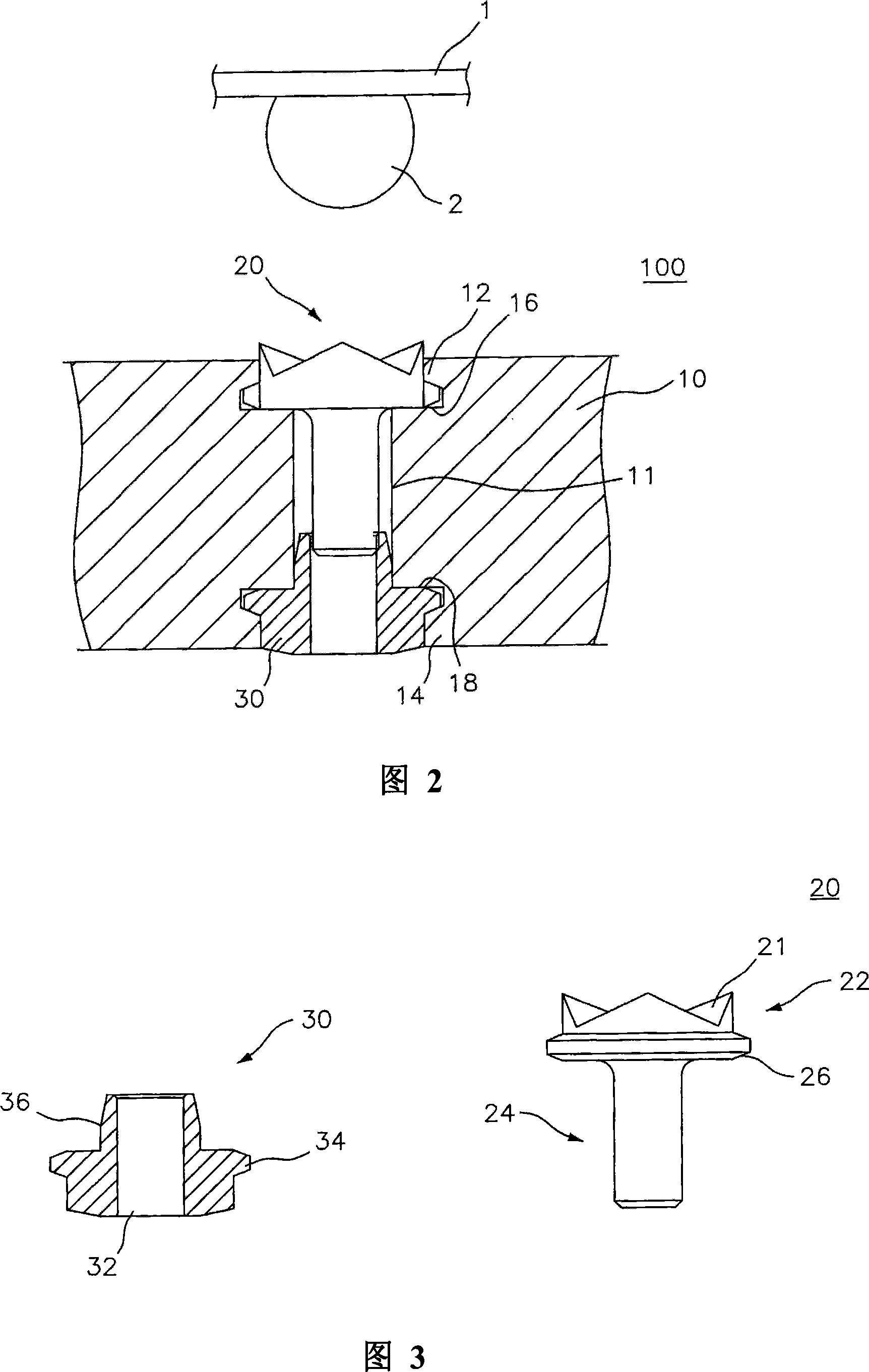
[0058] 2 is a cross-sectional view of a test probe device according to an embodiment of the present invention, and FIG. 3 is a cross-sectional view and a front view of a plunger and a contact pin according to an embodiment of the present invention.

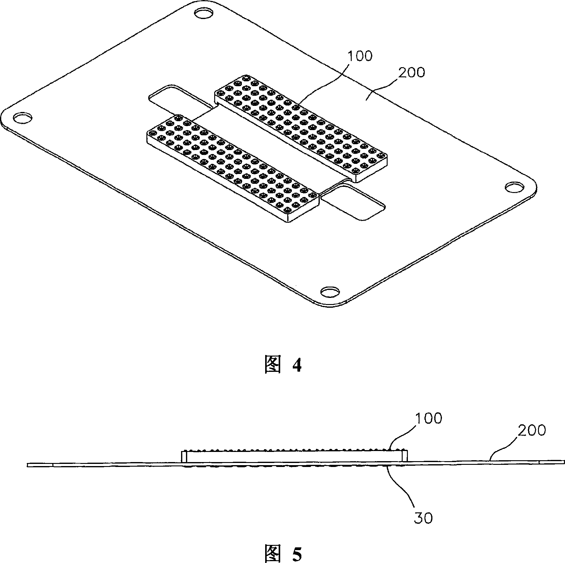
[0059] 4 and 5 are oblique views and front views of a test socket according to an embodiment of the present invention, and FIG. 6 is a bottom view and a partially enlarged view of an elastic plate according to an embodiment of the present invention.

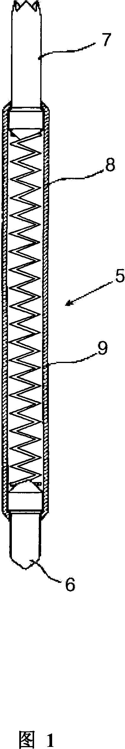
[0060] As shown in FIG. 2 , the test probe device includes: a plunger 20 contacting a contact terminal of a test object 1 ; an elastic plate 10 ; and a contact pin 30 between which an elastic member can be combined.

[0061] The elastic plate 10 is made of a non-conductive material and has a flat plate shape, and has a through hole 1...


PUM


Abstract

The invention relates to a contact probe and socket for testing semiconductor chips. The contact probe for testing semiconductor chips, comprises: a nonconductive elastic plate having main through-holes corresponding to contact terminals of a test target; plungers coupled on upper sides of the main through-holes, each having a plunger head that is elastically supported by the elastic plate and a plunger body that extends downwards from a center of the plunger head; and contact pins coupled on lower sides of the main through-holes, each having a receiving hole contacting the plunger body of each plunger at a center thereof. Thus, the contact probe employs a simple structure capable of coupling the plungers to the nonconductive elastic plate and elastically supporting the plungers, so that they can be easily manufactured, improve the signal pass of test electric current to secure test reliability, and be manufactured at a subminiature size suitable for equipment for testing semiconductor chips, which are gradually becoming complicated due to technical development.

Description

technical field [0001] The invention relates to a test probe device, in particular to a semiconductor chip test probe device and a test socket which are combined with an elastic plate made of non-conductive material and a plunger. Background technique [0002] The chip is an integrated circuit that performs various functions through the logic elements on the surface of the thin and small engraved board, and the electrical signals from the printed circuit board are transmitted through the bus (Bus) to perform the above functions. [0003] Generally speaking, there are many chips installed in various electronic products, and these chips are enough to determine the performance of electronic products. [0004] A printed circuit board (PCB: printed circuit board) is formed by using conductive copper to form circuit wiring on a thin substrate made of an insulator such as epoxy or phenolic resin and coating it. Integrated circuits, resistors or Electrical components such as switch...

Claims


Application Information

Patent Timeline
Patent Type & Authority Applications(China)
IPC IPC(8): G01R1/067G01R1/02G01R31/28H01L21/66
CPCG01R1/06733G01R1/0735G01R1/067
Inventor 李彩允
Owner LEENO IND INC
Why Eureka
Try Eureka