
Manufacture process of high precision alloy fled rheostat

An alloy resistor, high-precision technology, applied in resistors, resistor manufacturing, circuits, etc., can solve the problem of difficulty in ensuring the accuracy of the resistance value of alloy chip resistors, size deviation of alloy chip resistors, and different lengths of alloy chip resistors. problems, to achieve the effect of improving production yield, improving quality stability, and reducing punching and shearing burrs

Active Publication Date: 2008-02-06
PROSPERITY DIELECTRICS
View PDF0 Cites 8 Cited by
  • Summary
  • Abstract
  • Description
  • Claims
  • Application Information

AI Technical Summary

Problems solved by technology

Therefore, once the strip is broken, it represents the loss of an alloy chip resistor
[0005] In addition, in the process of making the high-precision alloy resistors, stamping and shearing must be carried out at the joints of the alloy chip resistors to separate them into single alloy chip resistors. In this process, improper stamping and shearing , that will cause the size deviation of more than two alloy chip resistors at the same time (that is, cause the length of each alloy chip resistor to be different), and it will be difficult to ensure that the resistance value accuracy of each alloy chip resistor falls within within a specific required tolerance range

Method used


Image

  • Manufacture process of high precision alloy fled rheostat
  • Manufacture process of high precision alloy fled rheostat
  • Manufacture process of high precision alloy fled rheostat

Examples


Embodiment Construction

[0027] The specific embodiment that the present invention adopts will be further described by the following embodiments and accompanying drawings:

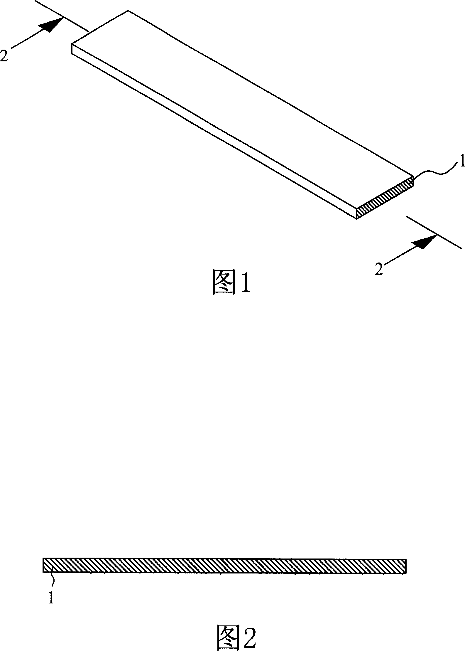
[0028] Please refer to FIG. 1 , which shows a perspective view of the first alloy plate prepared in the present invention. Fig. 2 is a cross-sectional view of section 2-2 in Fig. 1; the alloy plate 1 is formed by an alloy plate in the form of an extended strip, so it has a length extending direction, and the selection of its material and the determination of its thickness are based on the requirements Depending on the resistance value, for example, the material of the alloy plate can be nickel, chromium, manganese, aluminum, copper and other alloy plates.

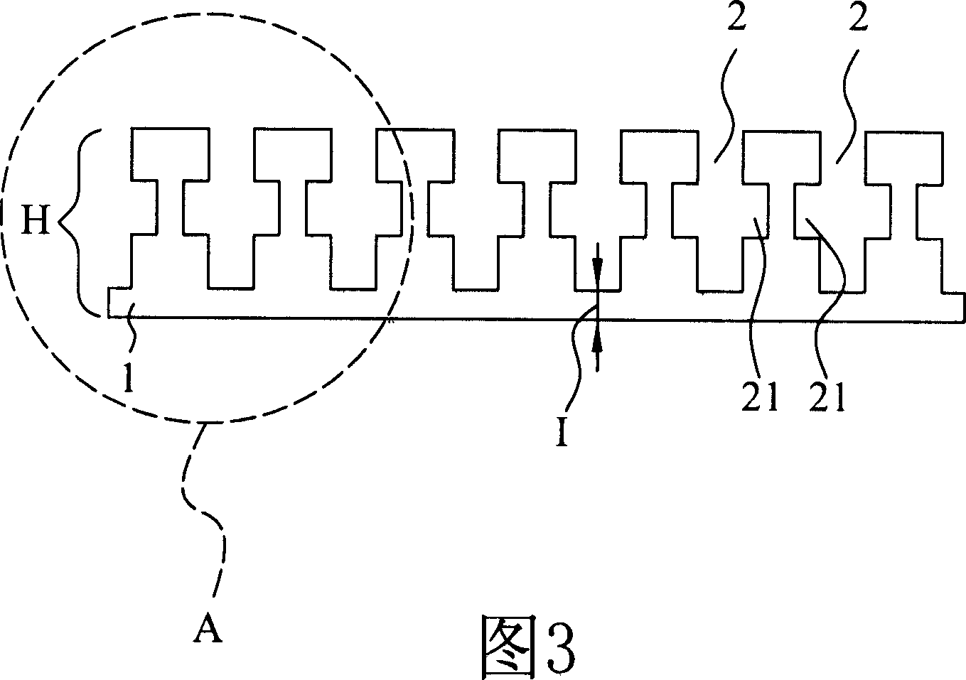
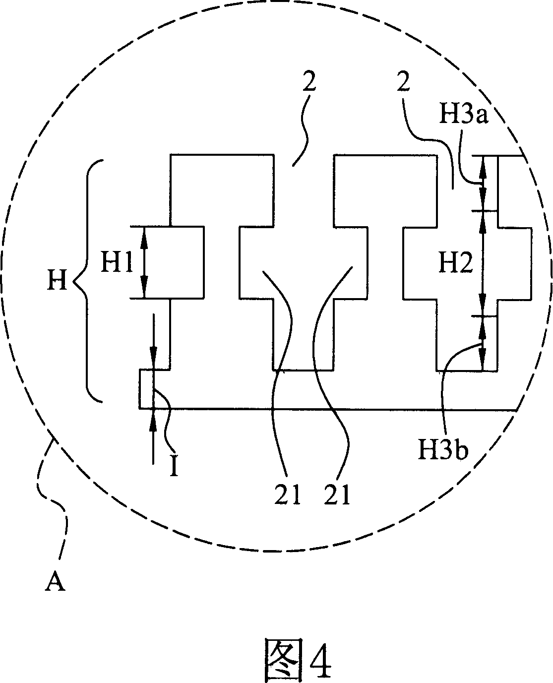
[0029] Please refer to Fig. 3 and Fig. 4. Fig. 3 and Fig. 4 show the schematic diagram and the enlarged view of some components after the alloy plate is stamped according to the required resistance value of the present invention. As shown in the figure, according to the require...


PUM


Abstract

A high-precision alloy resistor manufacturing process is to carry the dieing of a lengthy alloy board according to a predetermined shape so as to form a plurality of alloy resistance sections of the alloy board. The alloy resistance sections are arranged at intervals in the lengthy direction and the intervals are connected by residual material strips of the alloy board. Of the alloy resistance sections of the alloy board, an insulating section and two alloy board exposed section are underlined so as to form an anti-electroplating printing layer on the insulating section and to plate an electric conducting layer on the surface of the alloy board exposed sections. Afterwards, the anti-electroplating printing layer is removed and the surface of the alloy board exposed sections of each alloy resistance section is plated with an electric conducting layer, and the insulating section is molded with plastics. At last, each alloy resistance section is died and separated, thus forming a plurality of alloy resistance monomers.

Description

technical field [0001] The invention relates to a manufacturing process of a high-precision alloy resistor. An alloy plate is stamped according to a predetermined shape, combined with an anti-plating printing layer, plated a conductive layer, removes the anti-plating printing layer, trimming, plastic resin injection molding, die separation, electroplating Copper terminal material and other steps to complete the chip resistor manufacturing process. Background technique [0002] Traditional surface-mount chip resistors are generally manufactured by a thick-film printing process, which is mainly formed on a selected ceramic substrate through a sequence of printing, laser trimming, copper terminals, and electroplating processes. Resistor. In another type of resistor, it is the widely used alloy chip resistor. [0003] However, when manufacturing resistors with traditional thick-film printing process technology, it is difficult to achieve stable characteristics such as alloy ma...

Claims


Application Information

Patent Timeline
Patent Type & Authority Applications(China)
IPC IPC(8): H01C17/00
Inventor 陈桂成徐松宏张永发曾耀震
Owner PROSPERITY DIELECTRICS
Learn More