Dentritic pattern compound, preparation method and application
A compound and dendritic technology, applied in the field of dendritic compounds, can solve problems such as reducing carrier transport performance, and achieve good application prospects, high luminous brightness and efficiency, and high yield
- Summary
- Abstract
- Description
- Claims
- Application Information
AI Technical Summary
Problems solved by technology
Method used
Image
Examples
Embodiment 1
[0056] The synthetic routes of the three compounds involved in the present invention are shown in the following formula
[0057]
[0058] First prepare the precursor 4,4'-bis(2,3,4,5-tetraphenyl)-phenylbenzophenone
[0059] Response i:
[0060] 4,4'-dibromodiphenyl diketone (3.68g, 0.01mol), trimethylsilylacetylene (2.36g, 0.024mol), catalyst Pd (PPh 3 ) 2 Cl 2 (10%) and CuI (5%) toluene / triethylamine (1:1) 40ml, stirred at 60° C. for 12 hours under a nitrogen atmosphere, and after the reaction was completed, the solvent was distilled off under reduced pressure. The obtained solid product was purified by a silica gel column, and the yellow solid obtained after removing the solvent was 4,4'-bis-(trimethylsilylethynyl)-phenylbenzophenone. 4,4'-bis-(trimethylsilylethynyl)-phenylbenzophenone (2.01g, 0.005mol) and K 2 CO 3 (6.9g, 0.05mol) was stirred in 50mL of dichloromethane at room temperature for 6 hours. After the reaction was completed, it was washed with water, and th...
Embodiment 2
[0072] Preparation of OLEDs devices:
[0073] The first step: cleaning of tin indium oxide (ITO) glass
[0074] The ITO glass was washed with detergent, tap water, deionized water, acetone, and absolute ethanol in sequence, and then dried in an oven.
[0075] The second step: vapor deposition of organic semiconductor layer
[0076] Place the cleaned ITO glass slide in a vacuum chamber at 4×10 -4 Under the vacuum of Pa, each organic layer was vapor-deposited at a rate of 2 mm / s. The total thickness of the organic semiconducting layers in the device is ~100 nm.
[0077] Step 3: Cathode Preparation
[0078] An Al cathode is evaporated on the ITO substrate on which the organic layer has been evaporated, with a thickness of 100 nm.
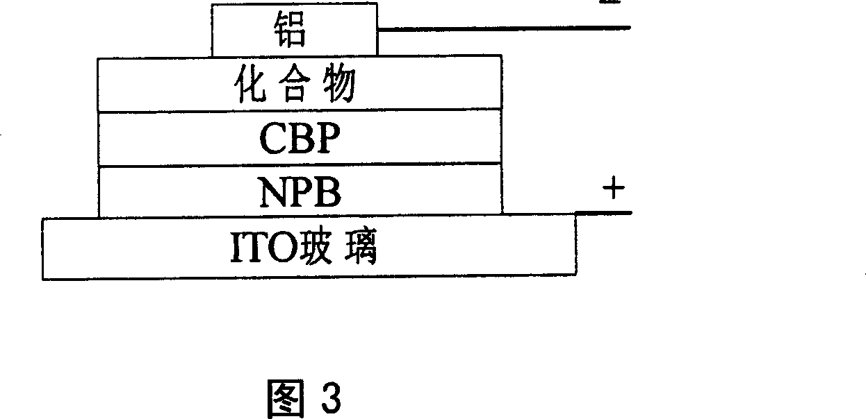
[0079] The fabricated device structure is shown in Figure 3.
[0080] Step 4: Testing of Device Performance
PUM
 Abstract
Description
Claims
Application Information
 - R&D
- Intellectual Property
- Life Sciences
- Materials
- Tech Scout
- Unparalleled Data Quality
- Higher Quality Content
- 60% Fewer Hallucinations
Browse by: Latest US Patents, China's latest patents, Technical Efficacy Thesaurus, Application Domain, Technology Topic, Popular Technical Reports.
© 2025 PatSnap. All rights reserved.Legal|Privacy policy|Modern Slavery Act Transparency Statement|Sitemap|About US| Contact US: help@patsnap.com


