Imaging apparatus and method of manufacturing the same

A camera device and manufacturing method technology, applied in the direction of image communication, camera body, color TV parts, etc., can solve the problems of difficult device scale, miniaturization, and difficulty in manufacturing camera devices, and achieve the effect of reliable occlusion

Active Publication Date: 2009-09-16
OLYMPUS CORP
View PDF4 Cites 0 Cited by
  • Summary
  • Abstract
  • Description
  • Claims
  • Application Information

AI Technical Summary

Problems solved by technology

[0007] However, in the above-mentioned conventional imaging device 101, unnecessary external light other than the light from the subject is blocked by blocking the area other than the light-receiving area 103d of the cover glass 102b. The dimensions (length×width×depth) of the recessed engaging portion of the upper light-shielding wall 103c are as close as possible to the external dimensions (length×width×thickness) of the glass cover 102b. When the light-shielding wall 103c is engaged on the glass cover 102b , so that there is almost no gap between the engaging part of the light shielding wall 103c and the glass cover 102b
For this reason, when the light-shielding wall 103c is engaged on the 102b, the position of the engaging portion of the light-shielding wall 103c must coincide with the position of the glass cover 102b with high precision, and it is often difficult to install the optical system formed with such a light-shielding wall on the solid-state imaging device, so there is a problem that it is difficult to manufacture an imaging device
[0008] In addition, there is a problem that preparing an optical system for forming such a light-shielding wall on each solid-state imaging element in order to correspond to the outer dimensions of the cover glass, that is, the chip size of the semiconductor chip of the solid-state imaging element, is very time-consuming and laborious.
Furthermore, due to the existence of the above-mentioned light-shielding wall, there is also a problem that the imaging device itself is enlarged.
For this reason, an endoscope device or a capsule endoscope incorporating such an imaging device tends to increase the size of the housing due to the imaging device, making it difficult to reduce the size of the device.

Method used


Image

  • Imaging apparatus and method of manufacturing the same
  • Imaging apparatus and method of manufacturing the same
  • Imaging apparatus and method of manufacturing the same

Examples


Embodiment approach 1

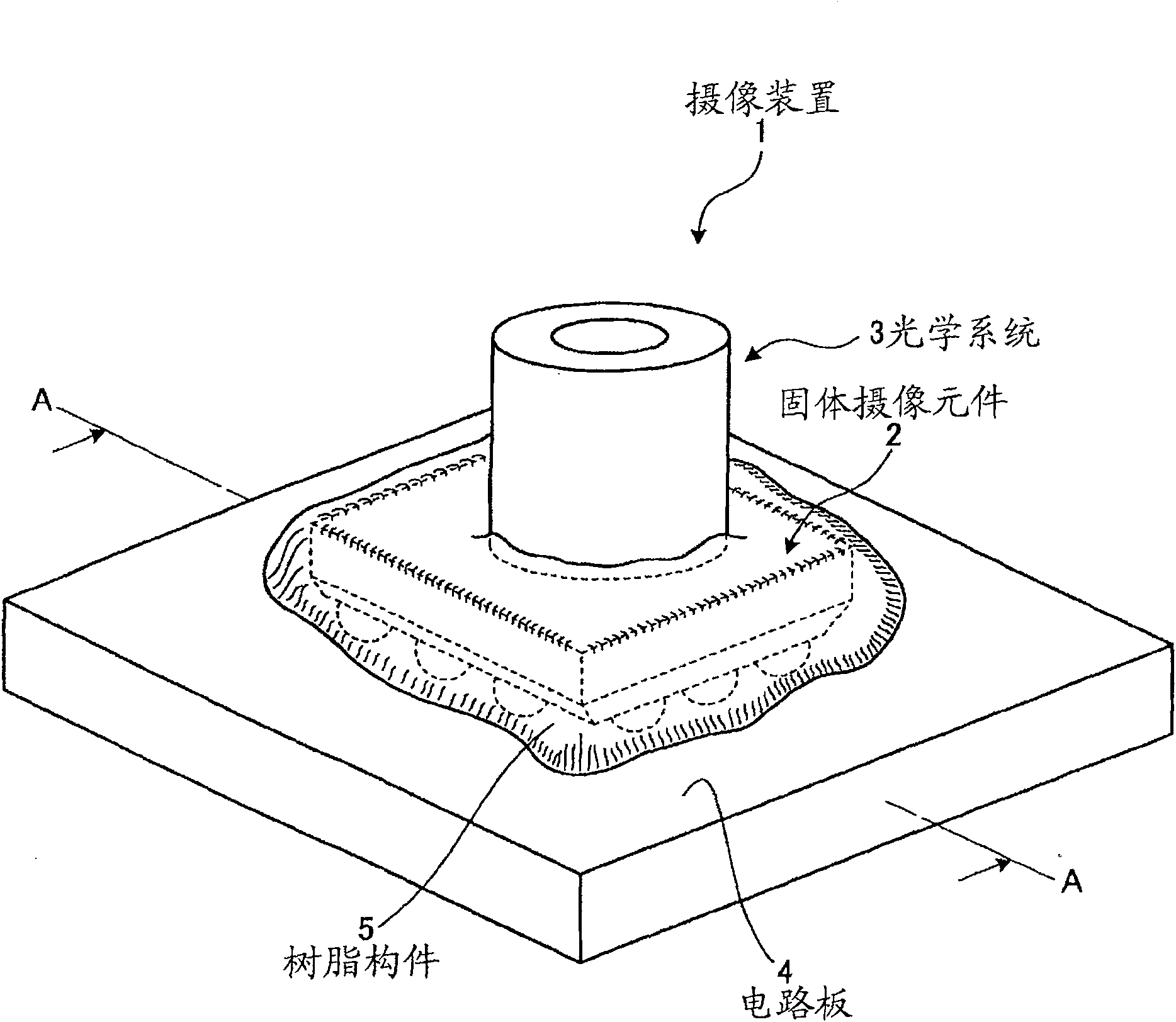
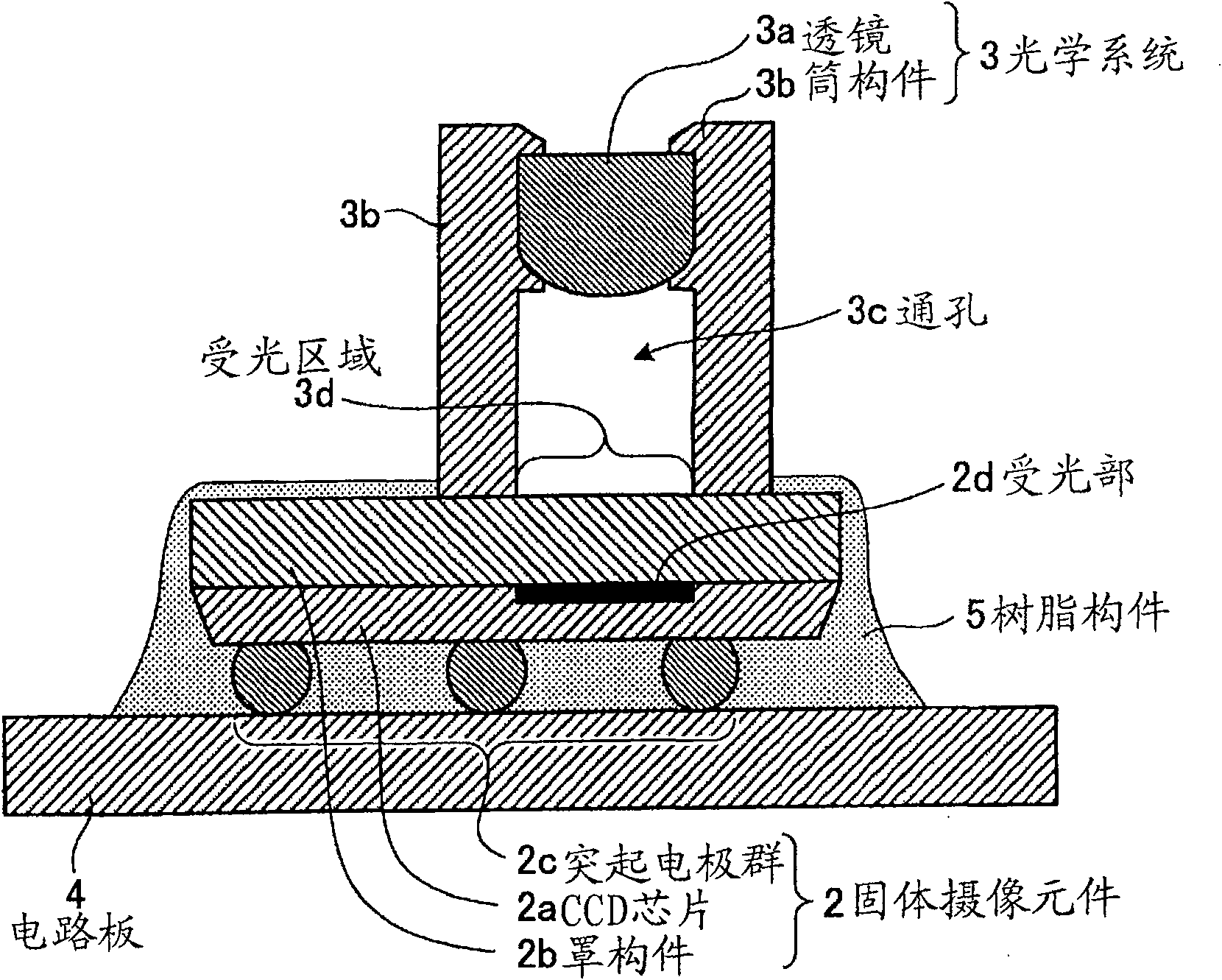
[0066] figure 1 It is a perspective view schematically showing a configuration example of the imaging device according to Embodiment 1 of the present invention. Such as figure 1 As shown, the imaging device 1 has: a solid-state imaging element 2, which receives light from an object and performs photoelectric conversion on the light to capture an image of the object; an optical system 3, which converges the light from the object On the light-receiving surface of the solid-state imaging element 2; the circuit board 4, which installs the solid-state imaging element 2; Areas other than those described above) are shaded.

[0067] Specifically, the package form of the solid-state imaging device 2 is a CSP type solid-state imaging device, the optical system 3 is provided on the upper surface, and the circuit board 4 is mounted on the lower surface side. Further, in the solid-state imaging device 2 mounted on the circuit board 4 in this way, the outer region of the installation r...

Embodiment approach 2

[0087] Next, Embodiment 2 of the present invention will be described. In the imaging device according to Embodiment 2, a positioning portion is formed on the cylindrical member of the optical system provided on the upper surface of the solid-state imaging element, and the positioning of the solid-state imaging element is determined by the positioning portion. Location.

[0088] Figure 4 It is a perspective view schematically showing a configuration example of the imaging device according to Embodiment 2 of the present invention. Figure 5 is illustrative Figure 4 B-B sectional schematic diagram of the side sectional structure of the imaging device shown. Such as Figure 4 , Figure 5 As shown, this imaging device 21 has an optical system 23 instead of the optical system 3 of the imaging device 1 of Embodiment 1 described above. The other configurations are the same as in Embodiment 1, and the same reference numerals are attached to the same configuration parts.

[0089...

Embodiment approach 3

[0095] Embodiment 3 of the present invention will be described below. This third embodiment realizes a capsule endoscope in which the imaging device 1 of the above-mentioned first embodiment is incorporated in a capsule-shaped housing.

[0096] Figure 9 It is a schematic cross-sectional view schematically illustrating a capsule endoscope incorporating the imaging device 1 according to Embodiment 1 of the present invention. Such as Figure 9 As shown, the capsule endoscope 201 has a capsule-shaped housing 202 formed in a substantially cylindrical shape, the housing 202 has an optical hemispherical cover 202a formed of a transparent optical member at one end, and an opaque hemispherical cover at the other end. 202b. In addition, the capsule endoscope 201 includes an imaging mechanism unit for imaging the inside of a body cavity to obtain image data, a wireless communication mechanism unit for transmitting various information including the image data, and a power supply unit ...


PUM


Abstract

An object is to realize an imaging apparatus in which an optical system that focuses light from an object can be readily attached to a solid-state imaging sensor, and in which an unnecessary external light other than the light from the object can be blocked without fail. An imaging apparatus of the present invention includes a solid-state imaging sensor (2) that receives the light from the object and performs photoelectric conversion, an optical system (3) that focuses the light from the object, and a resin material (5). The solid-state imaging sensor (2) has a semiconductor chip which receives the light from the object through a light receiving surface and performs the photoelectric conversion. A translucent member is provided on an upper surface of the semiconductor chip and electrode terminals is provided on a lower surface of the semiconductor chip. The optical system (3) is provided on a light receiving region on a surface of the translucent member. The light receiving region faces the light receiving surface. The resin material (5) reinforces a bonding strength of a circuit board (4) on which the solid-state imaging sensor (2) is placed and the group of electrode terminals of the solid-state imaging sensor (2), and shields a region outside the light receiving region of the translucent member from light.

Description

technical field [0001] The present invention relates to an imaging device that receives light from a subject and performs photoelectric conversion to capture an image of the subject, and a method of manufacturing the imaging device. Background technique [0002] Conventionally, there have been proposed small imaging devices built in portable terminals such as mobile phones and PDAs (Personal Digital Assistants) having imaging functions, including digital still cameras and video cameras. This imaging device has a function of receiving light from a subject, photoelectrically converting the received light, and capturing an image of the subject. Such an imaging device is realized using a solid-state imaging device such as a CCD or a CMOS image sensor, and an optical system for imaging light from a subject on a light-receiving surface of the solid-state imaging device (for example, refer to Patent Document 1). [0003] In addition, in recent years, such imaging devices have been...

Claims


Application Information

Patent Timeline
Patent Type & Authority Patents(China)
IPC IPC(8): H04N5/225H04N5/335H01L27/14H04N5/369
CPCH01L31/0203H01L27/14618H04N5/2254H04N2005/2255G03B17/02H01L27/14625H04N5/2257H04N5/2253H01L2224/16225H01L2224/32225H01L2224/73204H04N23/54H04N23/555H04N23/57H04N23/55H01L2924/00H01L27/14H04N23/00
Inventor 藤森纪幸
Owner OLYMPUS CORP
Why Eureka
Try Eureka