Solar battery laser marking device
A solar cell and laser marking technology, used in laser welding equipment, welding equipment, metal processing equipment, etc., can solve the problems of inability to mark large-format thin-film batteries and special graphics, and achieve high work efficiency and stable laser power output. , the effect of reducing working hours
- Summary
- Abstract
- Description
- Claims
- Application Information
AI Technical Summary
Problems solved by technology
Method used
Image
Examples
example 1
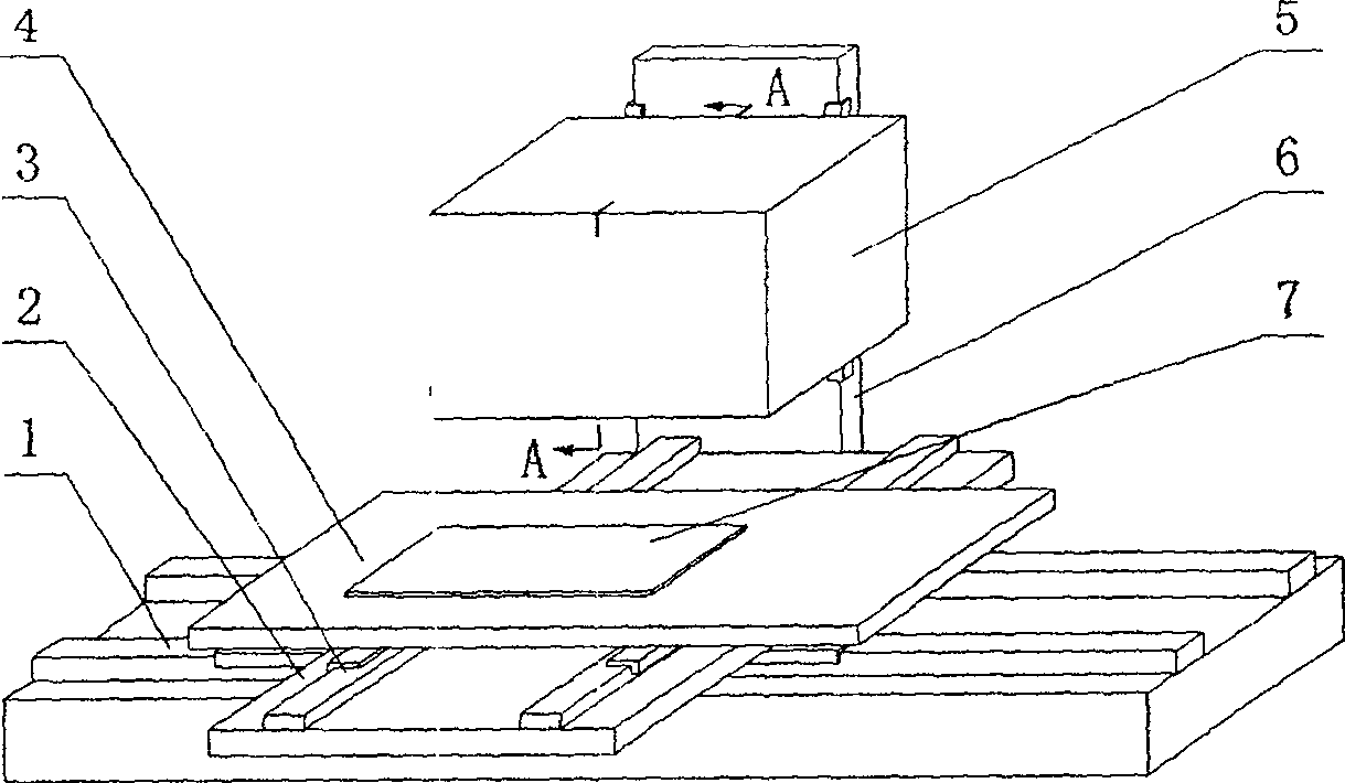
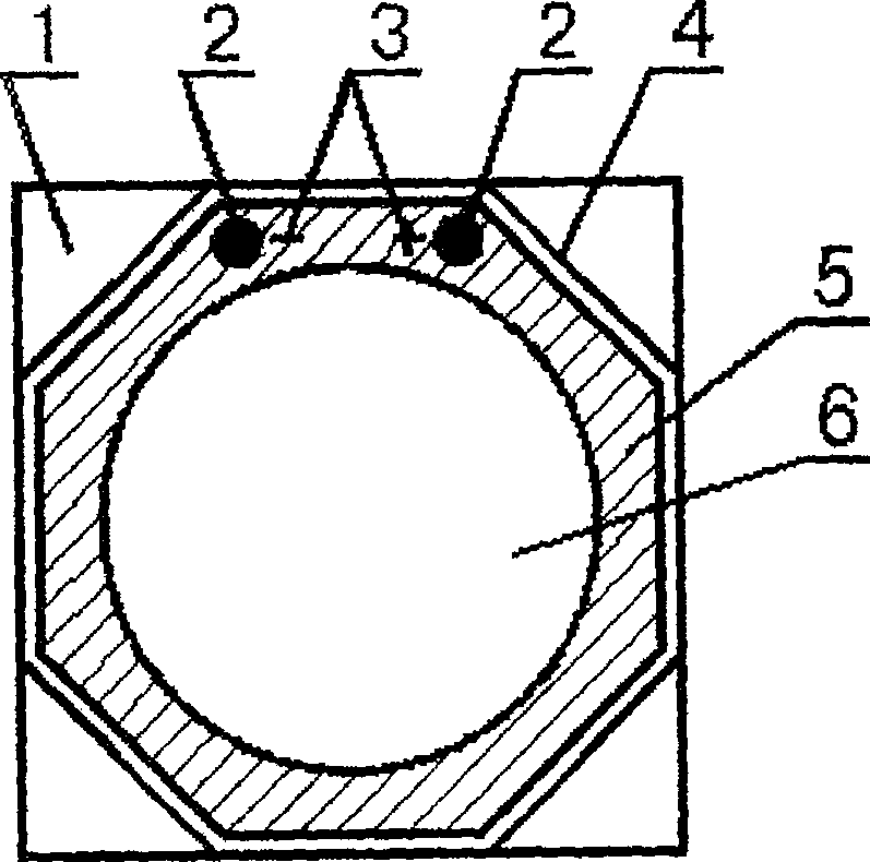
[0035]Example 1, on a substrate with a size of 355.6mm×406.4mm×0.7mm, the laser marking shape is a regular octagon with a circular transparent window in the middle of the single-format marking of a circular amorphous silicon thin-film solar cell (the workbench is not drawn, Same principle figure 1 )
[0036] Fabrication of the front electrode pattern: ITO, ZnO or SnO with a size of 355.6mm×406.4mm×0.7mm 2 The transparent conductive film is placed with the glass film side up on the Picture 1-1 In the No. 1 marking area, start the large-format infrared laser marking system, import the marking pattern of the front electrode of the battery, and set the marking range of the galvanometer scanning system to 360mm×410mm, using a single-format marking method , etch the continuous conductive film on the substrate into independent small pieces of required shape and size, such as Figure 4 The front electrode graph is shown in 7. The wavelength of the infrared laser is 1064nm, the la...
example 2
[0040] Example 2, embodiment figure 1 , m=2, n=4, same as above to produce amorphous silicon thin-film solar panels with unit cell spacing of 10mm and external dimensions of 1000mm×2000mm×3.0mm.
[0041] Front electrode graphic production: put the composite transparent conductive film glass film with a size of 1000mm×2000mm×3.0mm facing up, place it on the X-Y cross-linking work platform, start the large-format infrared laser marking system, and import the front electrode of the battery for marking Graphics, and set the marking range of the galvanometer scanning system to 500mm×500mm, divide the 1000mm×2000mm×3.0mm substrate to be marked into 8 marking areas of 500mm×500mm, and use multi-format marking method, marking 100 insulated isolation lines parallel to the long side with a spacing of 10mm on the continuous conductive film of the substrate, see Figure 7 The part shown in 1'. In this way, the continuous conductive film on the substrate is etched and divided into 100 re...
example 3
[0042] Example 3, see embodiment figure 1 , Laser marking amorphous silicon: Place the substrate film with the coated amorphous silicon photoelectric conversion layer facing down on the X-Y cross-linked loading platform, start the large-format green laser marking system, and import the battery amorphous silicon label Engraving graphics, and set the marking range of the galvanometer scanning system to 500mm×500mm, divide the 1000mm×2000mm×3.0mm substrate to be marked into 8 marking areas of 500mm×500mm, and use multi-format marking In the corresponding position of the front electrode pattern area on the deposited amorphous silicon substrate, the amorphous silicon layer is etched according to the design pattern requirements, and the continuous amorphous silicon film on the substrate is etched into 100 strips parallel to the long side. Marking lines with a spacing of 10mm expose the lead-out pattern of the front electrode, and the distance between the marking line engraved on amo...
PUM
| Property | Measurement | Unit |
|---|---|---|
| electrical resistance | aaaaa | aaaaa |
Abstract
Description
Claims
Application Information
 - R&D Engineer
- R&D Manager
- IP Professional
- Industry Leading Data Capabilities
- Powerful AI technology
- Patent DNA Extraction
Browse by: Latest US Patents, China's latest patents, Technical Efficacy Thesaurus, Application Domain, Technology Topic, Popular Technical Reports.
© 2024 PatSnap. All rights reserved.Legal|Privacy policy|Modern Slavery Act Transparency Statement|Sitemap|About US| Contact US: help@patsnap.com


