Modularized scanning probe microscope
A scanning probe and microscope technology, which is applied in the field of scanning probe microscopy, can solve the problems of reducing the contrast of scanning images, weak observation light, and inability to uniformly illuminate the field of view, achieving high resonance frequency and reducing costs
- Summary
- Abstract
- Description
- Claims
- Application Information
AI Technical Summary
Problems solved by technology
Method used
Image
Examples
Embodiment 1
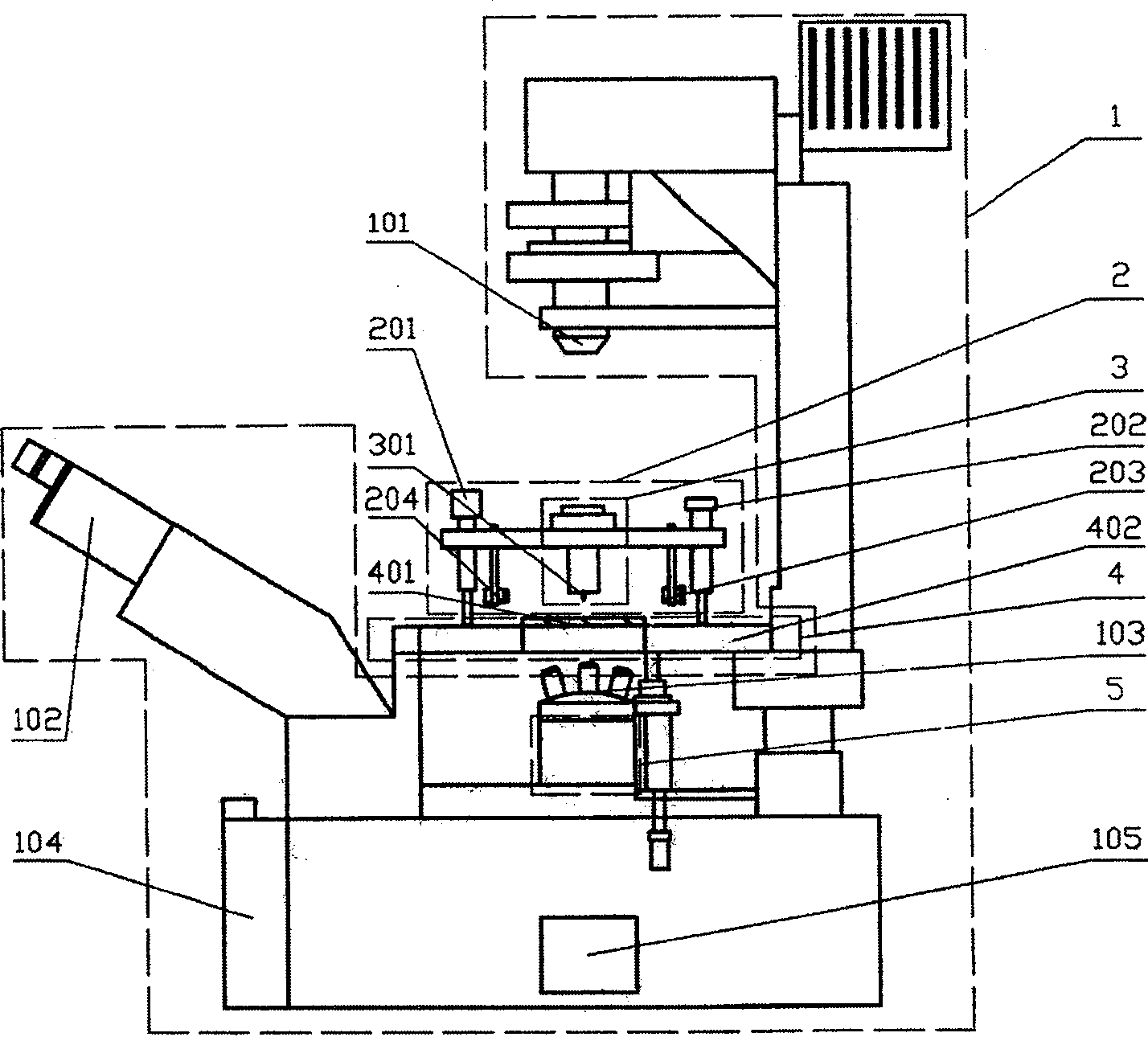
[0038] The principle schematic diagram of embodiment 1 is as Figure 5 As shown, the first module 1, the fourth module 4, and the fifth module 5 are combined. The first module 1 uses Nikon’s TE2000 universal biological microscope for research. This microscope has multi-port output design, ultra-precise Z-axis direction control and NIKON’s unique CFI60 optical system, and is equipped with new motorized accessories. Optional light sources and other accessories can be added to the far light path. The stray light elimination mechanism effectively blocks stray light and eliminates the influence of the surrounding temperature on the microscope prism, and has high anti-vibration performance. The fourth module 4 is a scanner 402 in xyz direction using P-733.3DD device of PI company, the scanning range is 30×30×10 μm, the center of the device is a 50×50 cm light hole, and the no-load resonance frequency is 1200 Hz. The sample is placed on the transparent sample stage of the fourth mod...
Embodiment 2
[0040] Embodiment 2 is a scanning near-field optical microscope, the principle schematic diagram is as Figure 6 As shown, the first module, the second module, the third module are used to scan the scanning head of the near-field optical microscope, and the fourth module is combined. The stepping motor 201 of the second module 2 adopts M-235.5DG of PI Company, and its one-way repeatability accuracy is 100nm; the lighting LED is fixed on the second module 2 and adjusted to irradiate the probe tip at a certain angle. The third module 3 is fixed on the second module 2, and the probe tip 301 is perpendicular to the surface of the sample. When working, the first module 1 completes the real-time observation of the needle tip and the sample at the micron level, the second module 2 completes the rough approximation, and the fourth module 4 completes the fine approximation and performs feedback tasks, and at the same time completes the scanning function.
Embodiment 3
[0042] The principle schematic diagram of embodiment 3 is as Figure 7 As shown, the first module, the second module, the third module scanning near-field optical microscope scanning head, and the fourth module are combined. The scanning near-field optical microscope scanning head includes a micro-cantilever probe tip 302, a first lens 303, the first reflector 304, the second reflector 305 and the second lens 306 place the sample on the transparent sample stage of the fourth module 4, and the third module 3 is driven by the second module 2 to roughly approximate the sample, and the fourth module 4 The X, Y, and Z three-dimensional flatbed scanners of module 4 approach and scan the sample in fine detail, thus forming an atomic force microscope for scanning the tip of the sample. The transmissive type illuminated below, because the scanner of module four has a light aperture.
PUM
 Abstract
Description
Claims
Application Information
 - Generate Ideas
- Intellectual Property
- Life Sciences
- Materials
- Tech Scout
- Unparalleled Data Quality
- Higher Quality Content
- 60% Fewer Hallucinations
Browse by: Latest US Patents, China's latest patents, Technical Efficacy Thesaurus, Application Domain, Technology Topic, Popular Technical Reports.
© 2025 PatSnap. All rights reserved.Legal|Privacy policy|Modern Slavery Act Transparency Statement|Sitemap|About US| Contact US: help@patsnap.com


