Circuit board air-pumping ink-penetrating hole-filling method and device thereof

An air extraction device and circuit board technology, which is applied in the manufacturing of electrical components, printed circuits, and multi-layer circuits, can solve the problems of covering electroplating structure depression, insufficient depth of ink filling holes, and poor production process yield, etc. The effect of ink sag difference and improving the yield of the manufacturing process

Inactive Publication Date: 2009-05-27
COMPEQ MFG
View PDF5 Cites 3 Cited by
  • Summary
  • Abstract
  • Description
  • Claims
  • Application Information

AI Technical Summary

Problems solved by technology

[0005] 1. Purely by screen printing, since the conductive hole 51 is a high-aspect-ratio hole type, the filling depth of the ink hole will be insufficient, and the hole cannot be filled with ink 100%, and a gap will appear on the ink-permeable surface 52 of the circuit board 50 , resulting in a depression 61 behind the platen (see Figure 11)
[0006] 2. If the conductive hole 51 is filled with ink by printing multiple times on the screen, the air bubble 60 will be squeezed into the hole during the multiple printing process, and the air bubble 60 near the hole of the circuit board 50 (as shown in Figure 10 As shown), it will lead to the defect of depression 61 or perforation 62 in the covering electroplating (Lid-Plating) structure (as shown in Figure 11 and Figure 12)
[0007] Aiming at the problem that the yield rate of the manufacturing process is relatively poor in the prior art when implementing the plug hole operation, the inventor has designed the method and device for pumping air through the ink plug hole of the present invention

Method used


Image

  • Circuit board air-pumping ink-penetrating hole-filling method and device thereof
  • Circuit board air-pumping ink-penetrating hole-filling method and device thereof
  • Circuit board air-pumping ink-penetrating hole-filling method and device thereof

Examples


Embodiment Construction

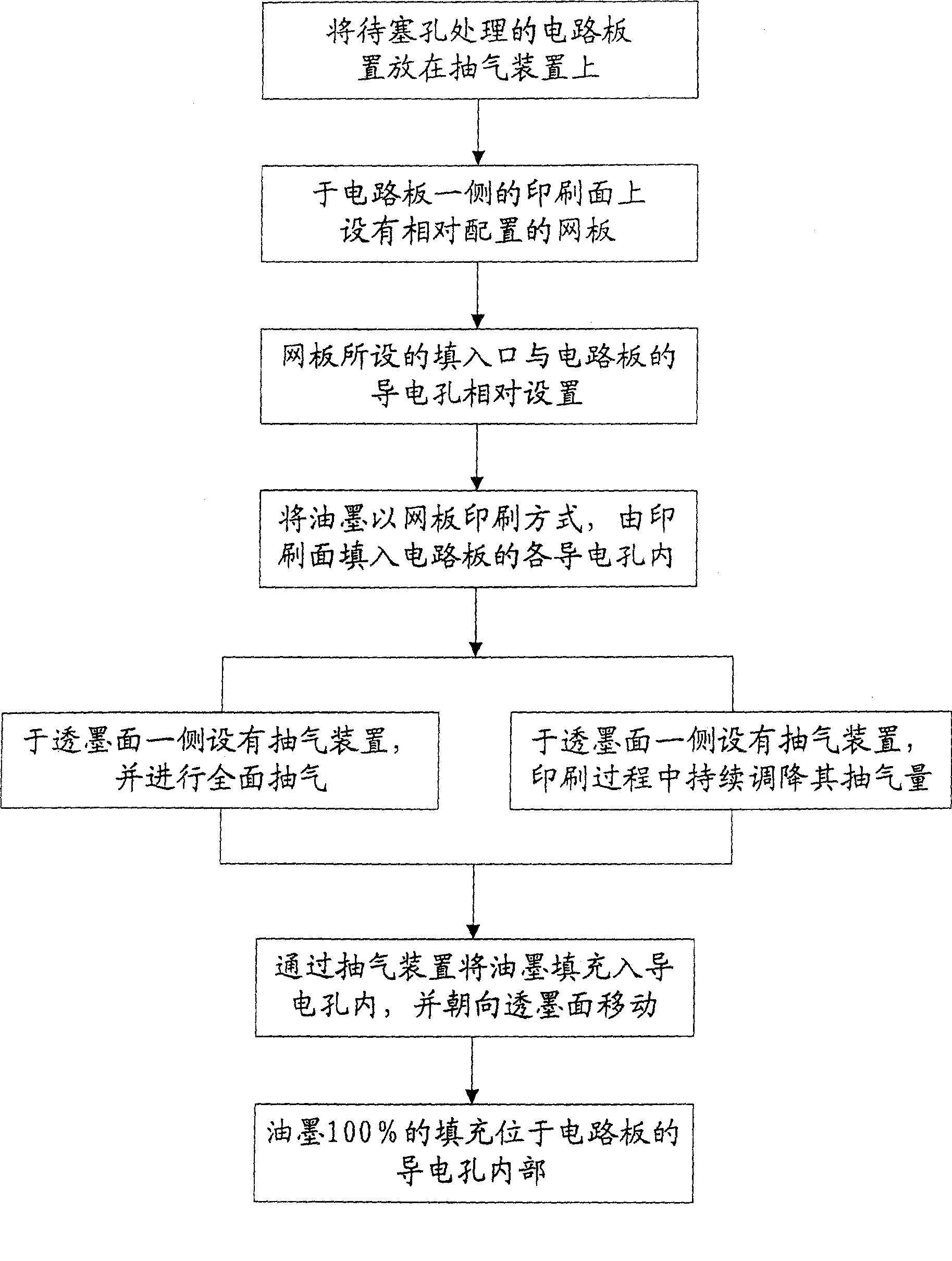
[0032] see figure 1 Shown, the circuit board air extraction method that the present invention proposes through ink plug hole, its method mainly contains:

[0033] a. Place the circuit board to be plugged on the air extraction device;

[0034] b. Set a stencil (or steel plate) on the printing surface opposite to the circuit board side;

[0035] c. The filling port set by the screen plate is set opposite to the conductive hole of the circuit board;

[0036] d. Then move the ink on the screen with a scraper, and the ink can enter the hole from the filling port through the conductive hole on the side of the printing surface;

[0037] e. After the suction device on the ink-permeable surface of the other side of the circuit board is activated, the ink in the printing surface and the conductive hole can be moved towards the ink-permeable surface to complete filling.

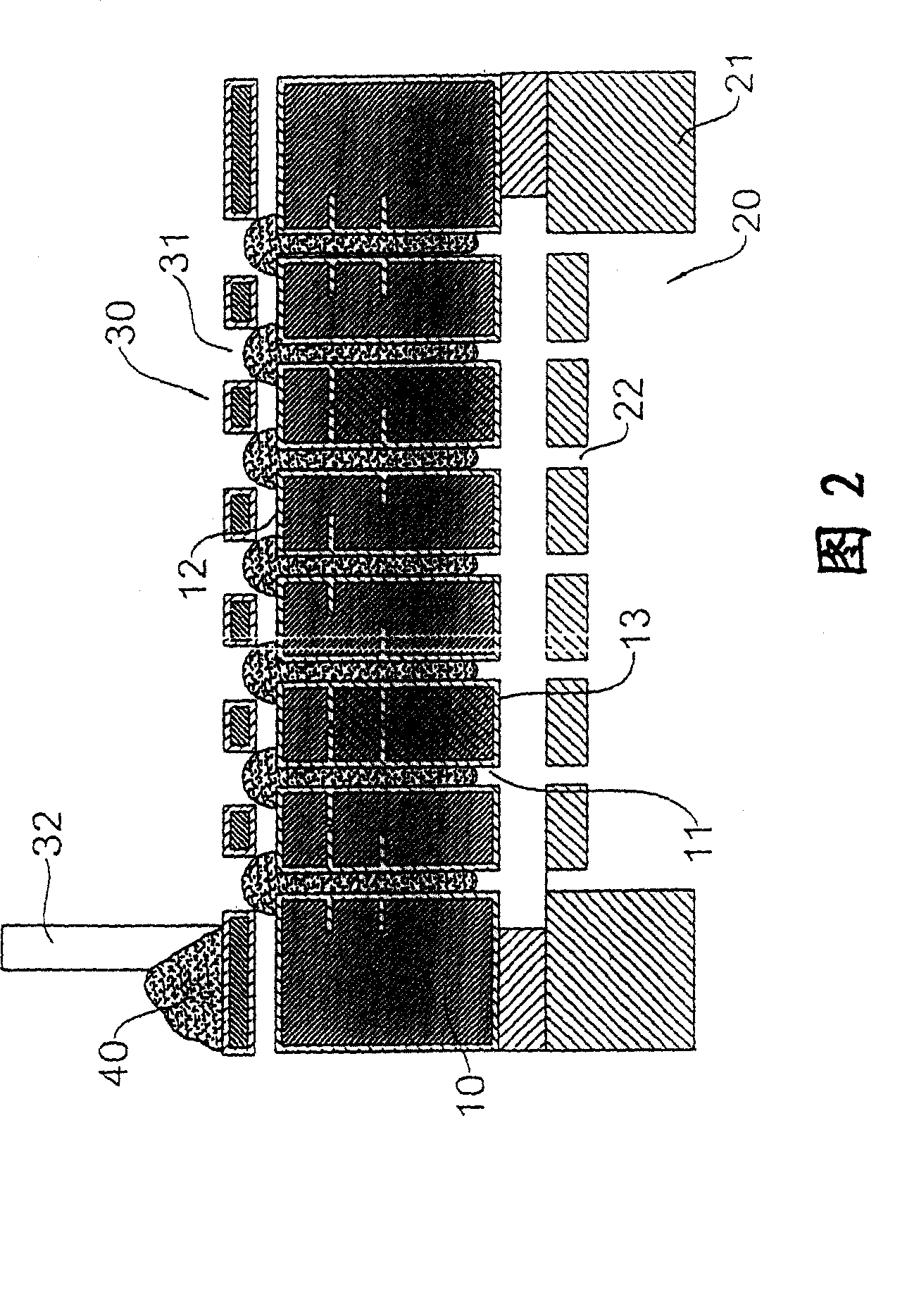
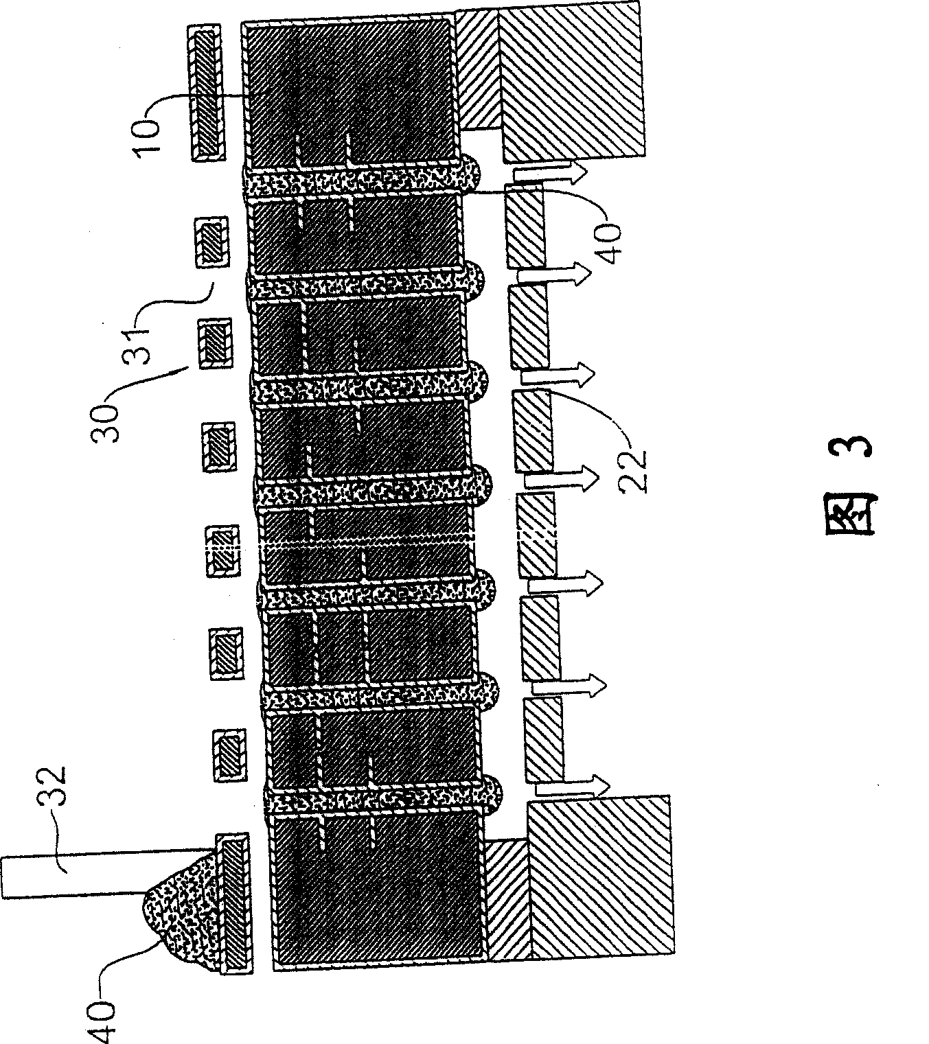
[0038] For the specific implementation method of the present invention, please refer to Fig. 2 and shown in Fig. 3...


PUM


Abstract

The invention discloses an air exhaustion ink penetration plug method of circuit board, and a relative device, wherein the upper and lower sides of a circuit board are respectively provided with a network plate and an air absorber, the network plate is provided with a stuff inlet relative to a conductive hole of the circuit board, and the invention uses network plate print method to stuff ink into the conductive hole, and engaged with the exhaustion of an exhauster to fill ink completely into the conductive hole, therefore, the conductive hole with high length / width ratio can avoid foam, concave or break, to improve quality.

Description

technical field [0001] The present invention relates to a circuit board manufacturing process and its device, in particular to a method for pumping and ink-permeable plug holes used in the production of circuit boards, in which ink is filled into the conductive holes of the circuit board during the production process. and its devices. Background technique [0002] At present, in order to meet the needs of different products produced, the circuit boards produced have been developed to the design and application of multi-layer boards. Between the unit boards of each layer of the multi-layer circuit board, in order to provide the electrical connection of the designed circuit, Therefore, relative perforations are provided on the unit board, and a conductive material (such as copper material, etc.) is provided on the edge of the perforation to form a conductive hole with a conductive effect. The conductive material of the conductive hole is connected to the circuit on each layer ...

Claims


Application Information

Patent Timeline
Patent Type & Authority Patents(China)
IPC IPC(8): H05K3/46H05K3/02
Inventor 杨伟雄白家华黄秀玲
Owner COMPEQ MFG
Why Eureka
Try Eureka