Temp regulator of semiconductor substrate

A temperature adjustment device and semiconductor technology, which is applied in the fields of semiconductor devices, semiconductor/solid-state device manufacturing, and semiconductor/solid-state device components, etc., can solve the problem of reduced uniformity of temperature distribution, slower cooling of semiconductor substrates, and inability of air to escape smoothly. and other problems, to achieve the effect of suppressing warpage, rotation and lateral dislocation

Inactive Publication Date: 2009-03-04
SMC CORP
View PDF4 Cites 1 Cited by
  • Summary
  • Abstract
  • Description
  • Claims
  • Application Information

AI Technical Summary

Problems solved by technology

As one of the measures, it is considered to reduce the gap forming parts when placing a high-temperature semiconductor substrate on the heat transfer plate of the temperature adjustment device whose temperature is adjusted to a predetermined temperature. However, in this case, due to the high cooling rate, the The resulting temperature change rate in the thickness direction of the substrate is different, therefore, a large temperature difference is generated between the lower surface and the upper surface of the semiconductor substrate, so warpage occurs on the substrate, and due to this warpage, there is a reduction in the uniformity of the temperature distribution , the problem that the cooling of the semiconductor substrate becomes slower
In particular, such warping is particularly noticeable on large-diameter semiconductor substrates, and has become a major problem in recent manufacturing processes that increase the diameter of semiconductor substrates.
[0005] In addition, when the semiconductor substrate becomes larger as described above, and the gap between the heat transfer plate on which it is placed becomes smaller, when the semiconductor substrate is placed on the heat transfer plate, the air between the substrate and the heat transfer plate cannot escape smoothly. As a result, there will be a problem that the semiconductor substrate placed on the heat transfer plate will be misaligned by rotation or lateral sliding, and measures must be taken for this problem.

Method used


Image

  • Temp regulator of semiconductor substrate
  • Temp regulator of semiconductor substrate
  • Temp regulator of semiconductor substrate

Examples


Embodiment Construction

[0025] Embodiments of the temperature adjusting device of the present invention will be described in detail below with reference to the accompanying drawings.

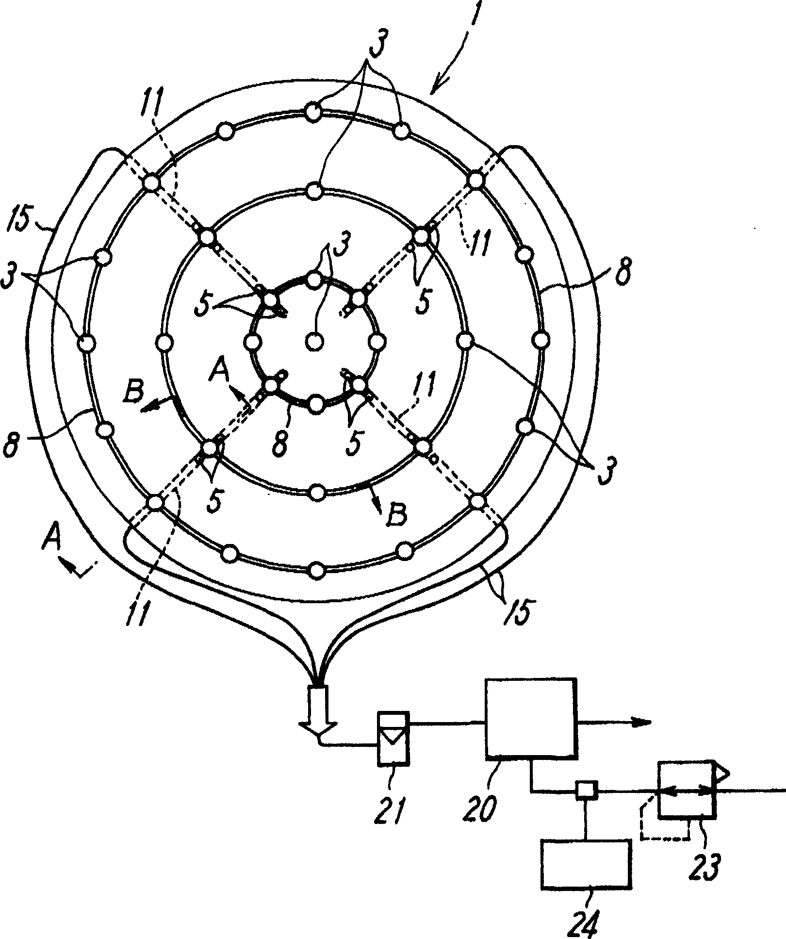
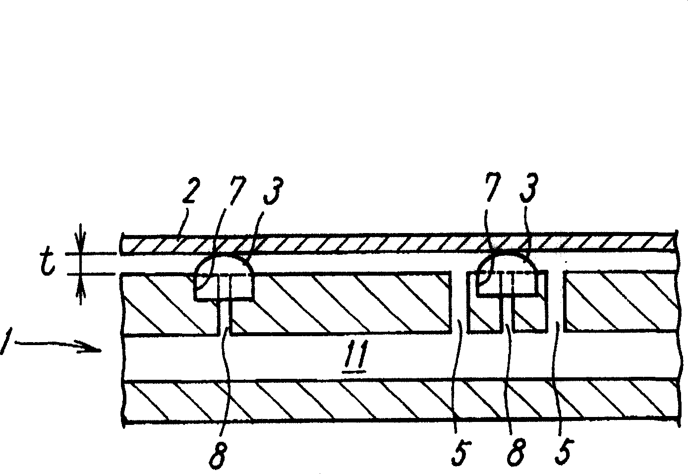
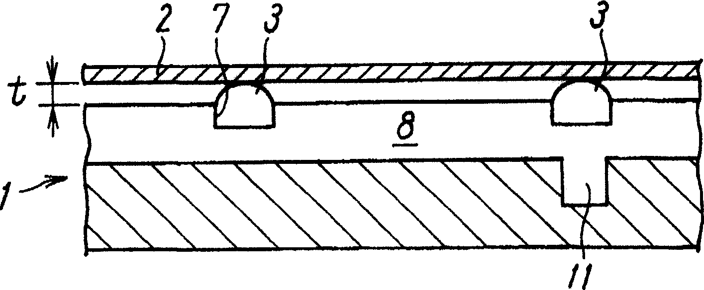
[0026] Figure 1-Figure 3 It is a diagram schematically showing a first embodiment in which the present invention is applied to a temperature control device for temperature control of a silicon wafer. The heat transfer plate 1 in the temperature regulating device, such as figure 2 and image 3 As shown, a silicon chip 2 is placed on it for heating or cooling to a specified temperature, and it also has a temperature regulating part, which is inside a surface plate made of a good thermal conductor aluminum or copper-based material Side mounts incorporate Peltier elements, etc.

[0027] On the surface of the heat transfer plate 1, in order to prevent particles from adhering to the silicon wafer 2, a plurality of gap-forming members 3 made of ceramics having hemispherical tops are discretely provided. The gap forming ...


PUM


Abstract

The purpose of this invention is to provide the heat conducting plate of a temperature adjusting apparatus rapidly cooling a semiconductor substrate without generating warpage in the semiconductor substrate during heating/cooling. Sucking holes connected to a vacuum source for sucking a silicon wafer are provided near proximity gaps in the heat conducting plate of the temperature adjusting apparatus for heating or cooling the silicon wafer. When the vacuum source performs sucking through the sucking holes, the silicon wafer is sucked to the heat conducting plate with a small gap being interposed between them, so that the warpage accompanying rapid heating/cooling is suppressed, and the wafer is uniformly cooled for a short period time.

Description

technical field [0001] The present invention relates to a temperature regulating device for a semiconductor substrate, and more particularly to a temperature regulating device having a heat transfer plate for heating and cooling a semiconductor substrate. Background technique [0002] Conventionally, temperature control devices for heating and cooling semiconductor substrates to predetermined temperatures have been widely used. [0003] This temperature adjustment device is composed of a heat transfer plate made of aluminum or copper-based materials with excellent heat transfer properties on which a semiconductor substrate is placed, and a heat source part in which a Peltier element or the like is incorporated (for example, refer to: Japanese Patent Application Laid-Open No. 2000 -306984). [0004] However, in recent years, in order to manufacture semiconductors cheaply, the diameter of the semiconductor substrate from which the semiconductor wafer is cut has been made as l...

Claims


Application Information

Patent Timeline
Patent Type & Authority Patents(China)
IPC IPC(8): H01L23/40H01L23/38H01L23/34H01L21/683H01L21/02H01L21/027H01L21/20H01L21/68
CPCH01L21/67103H01L21/67248
Inventor 财贺正生小野贵弘
Owner SMC CORP
Why Eureka
Try Eureka