Semiconductor device and data writing method therefor

A data writing, semiconductor technology, applied in semiconductor devices, semiconductor/solid-state device manufacturing, semiconductor/solid-state device components, etc., can solve problems such as inability to seek copyright protection

Inactive Publication Date: 2008-11-05
KK TOSHIBA
View PDF4 Cites 0 Cited by
  • Summary
  • Abstract
  • Description
  • Claims
  • Application Information

AI Technical Summary

Problems solved by technology

[0008] However, on the other hand, since data can be rewritten in this way, for example, by rewriting images, etc., it may not be possible to seek copyright protection.

Method used


Image

  • Semiconductor device and data writing method therefor
  • Semiconductor device and data writing method therefor
  • Semiconductor device and data writing method therefor

Examples


no. 1 approach

[0028] In the first embodiment, the configuration of an MRAM capable of preventing rewriting of data written once will be described.

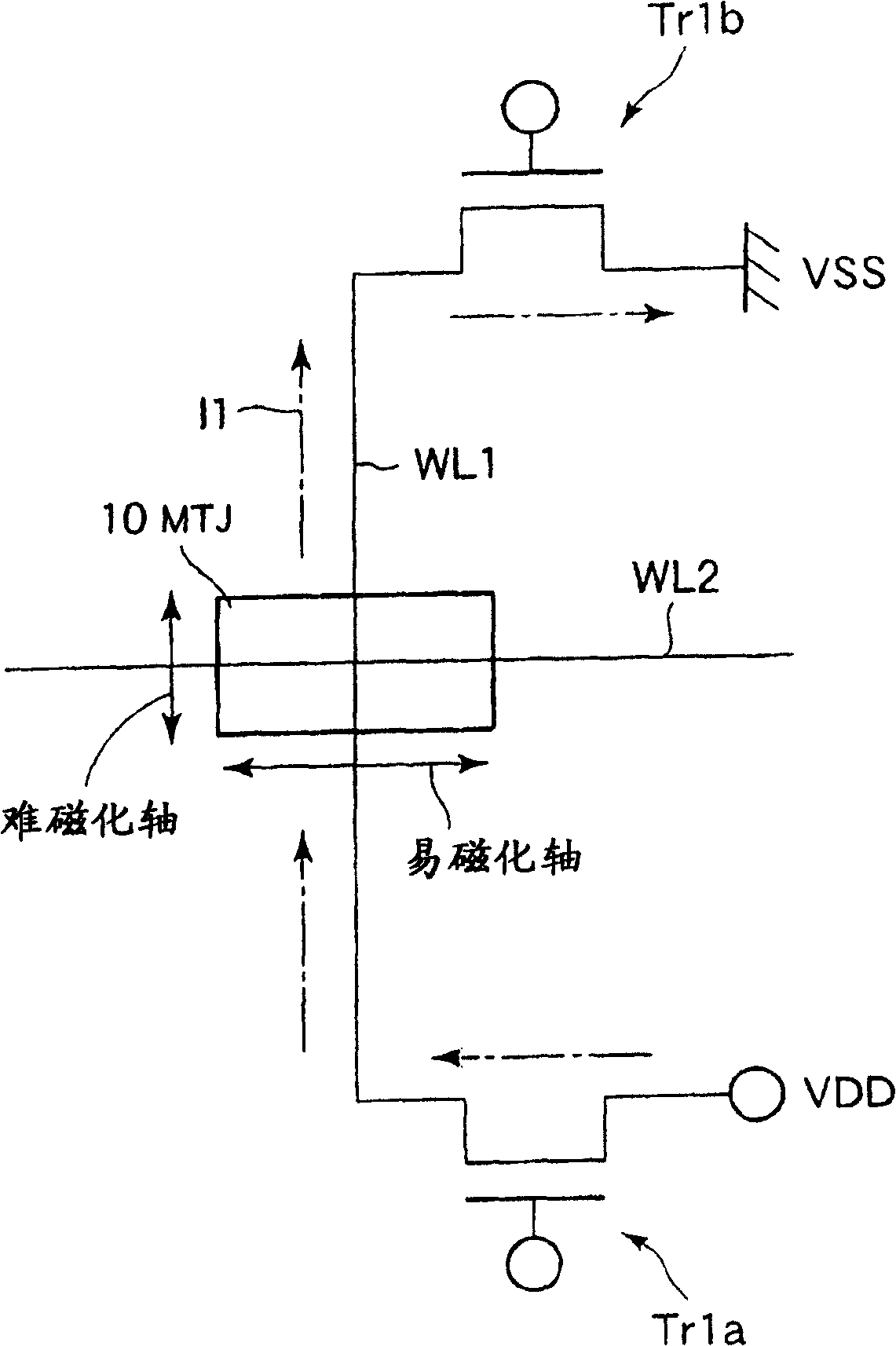
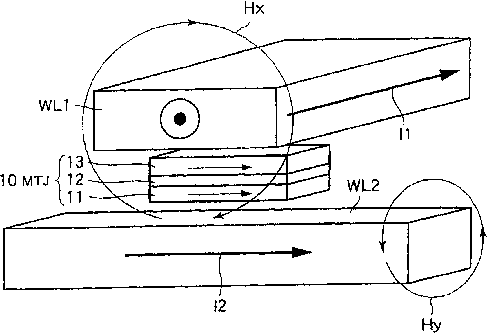
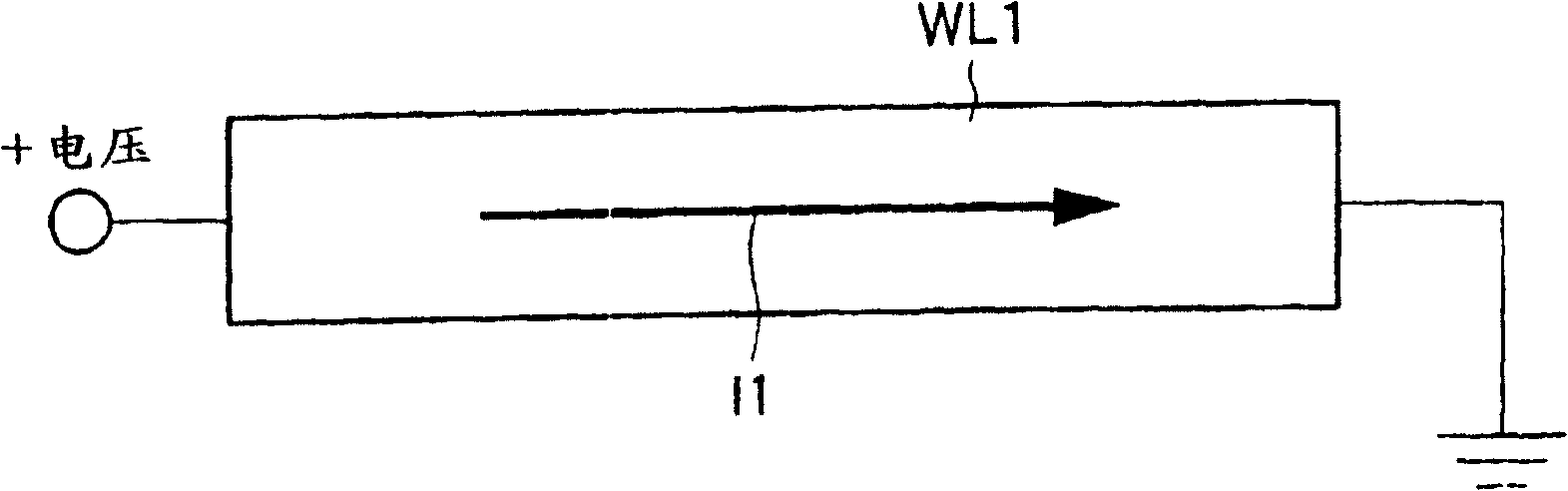
[0029] figure 1 and figure 2 A schematic circuit diagram and perspective view showing the MRAM according to the first embodiment of the present invention. image 3 Indicates the irreversible current direction of the first write wiring according to the first embodiment of the present invention.

[0030] Such as figure 1 and figure 2 As shown, in the storage unit, the first write wiring (such as a bit line) WL1 and the second write wiring (such as a word line) WL2 are arranged orthogonally to each other, and the MTJ element 10 is arranged on these first and second write wirings. At the intersection of WL1 and WL2. The MTJ element 10 is composed of a pinned layer 11 , a free layer (recording layer) 13 , and a tunnel insulating film 12 sandwiched between the pinned layer 11 and the free layer 13 .

[0031] Furthermore, the first write wir...


PUM


Abstract

A semiconductor device includes a memory portion in which a plurality of magneto-resistance effect elements each having a hard-axis of magnetization and an easy-axis of magnetization are arranged and one of binary data is written in all the magneto-resistance effect elements, and a circuit portion to which a write current is supplied to write only the other one of the binary data in only a selected magneto-resistance effect element selected from the magneto-resistance effect elements.

Description

technical field [0001] The present invention relates to a semiconductor device and a data writing method of the semiconductor device, in particular to a magnetic random access including an MTJ (Magnetic Tunnel Junction) element that stores "1" and "0" information by utilizing the tunnel magnetoresistance (TMR) effect Memory (MRAM). Background technique [0002] In recent years, magnetic random access memories (hereinafter referred to as MRAMs) using the tunnel magnetoresistance effect are expected to be high-speed and large-capacity storage media. [0003] In such MRAM, as Figure 10 and Figure 11 As shown, the first writing wiring (such as a bit line) WL1 and the second writing wiring (such as a word line) WL2 are arranged orthogonally to each other, and the MTJ element 10 is arranged at the intersection of these first and second writing wirings WL1 and WL2 superior. This MTJ element 10 is composed of a pinned layer 11 , a free layer (recording layer) 13 , and a tunnel ...

Claims


Application Information

Patent Timeline
Patent Type & Authority Patents(China)
IPC IPC(8): G11C11/15H01L43/08H01F10/32H01L21/8246H01L23/00H01L27/105H01L43/02
CPCB82Y25/00H01F10/3254G11C11/15
Inventor 梶山健
Owner KK TOSHIBA
Why Eureka
Try Eureka