Test key structure
A technology for testing keys and joints, which is applied in semiconductor/solid-state device testing/measurement, electrical components, electric solid-state devices, etc., and can solve problems such as the inability to know the influence of spacers
- Summary
- Abstract
- Description
- Claims
- Application Information
AI Technical Summary
Problems solved by technology
Method used
Image
Examples
no. 1 example
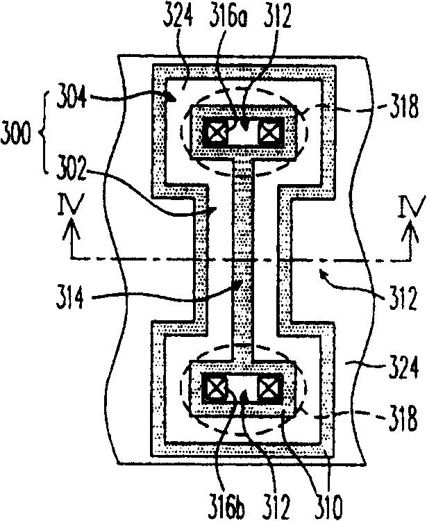
[0040] image 3 is a top view of the test key structure according to the first embodiment of the present invention, and Figure 4 Yes image 3 Schematic cross-section of the IV-IV line segment.
[0041] Please refer to image 3 and Figure 4 The test key structure of this embodiment includes a substrate 400, a closed loop 300, a spacer 310, a first doped region 312 and a second doped region 314, and contact windows 316a, 316b, wherein the closed loop 300 is, for example, a polysilicon layer. The aforementioned closed circuit 300 is located on the base 400, and has two wires 302 and two connecting parts 304, wherein each connecting part 304 is connected to one end of the wires 302 and surrounds a contact area 318, and the shape of this closed circuit 300 may include Dog-bone shape or other suitable shapes, and the wire 302 is not limited to a straight line, but can also be a curved line or a broken line. The spacer 310 is disposed on the edge of the closed loop 300 and cov...
no. 2 example
[0046] Figure 5 It is a top view of the test key structure according to the second embodiment of the present invention. Please refer to the following description for the structural differences between it and the first embodiment. and, Figure 5 The same reference numerals as those of the first embodiment are used in part of the drawings to denote the same components.
[0047] Please refer to Figure 5 , which includes a substrate 400, two wires 500, a spacer 310, a first doped region 312, a second doped region 314, and contact windows 510a, 510b. The wire 500 may be a polysilicon layer. Moreover, the two wires 500 are arranged side by side on the substrate 400, and have a middle portion 502 and two end portions 504, and the distance D1 between the middle portion 502 of each wire 500 is smaller than the distance D2 between the end portions 504 of each wire 500 . Moreover, the spacer 310 is disposed on the edge of the conductive wire 500 and covers the base 400 between the ...
PUM
 Abstract
Description
Claims
Application Information
 - R&D
- Intellectual Property
- Life Sciences
- Materials
- Tech Scout
- Unparalleled Data Quality
- Higher Quality Content
- 60% Fewer Hallucinations
Browse by: Latest US Patents, China's latest patents, Technical Efficacy Thesaurus, Application Domain, Technology Topic, Popular Technical Reports.
© 2025 PatSnap. All rights reserved.Legal|Privacy policy|Modern Slavery Act Transparency Statement|Sitemap|About US| Contact US: help@patsnap.com


