Semiconductor packer and production for godown chip

A package and semiconductor technology, which is applied to the field of stacked chip semiconductor packages and their manufacturing methods, can solve the problems of increasing the complexity of the overall packaging process, the required time course, the inconvenience of the process, and the increase in cost, so as to improve the heat dissipation efficiency. and electrical quality, reducing packaging costs and improving packaging efficiency

Inactive Publication Date: 2008-01-16
SILICONWARE PRECISION IND CO LTD
View PDF7 Cites 0 Cited by
  • Summary
  • Abstract
  • Description
  • Claims
  • Application Information

AI Technical Summary

Problems solved by technology

[0009] However, in order to meet the light, thin, short, small, and high-function requirements of electronic products, the size requirements of semiconductor packaging structures are getting smaller and smaller. Therefore, chip-scale packaging (Chip Scale Package, SP) structures, such as thin ball grid arrays The demand for package (TFBGA) is increasing, but because the chip-scale package (CSP) semiconductor package emphasizes that the size of the substrate is equivalent to the size of the chip, and the area for chip wire bonding can only be formed in the area for chip bonding ( Die-Attaching Area) to the edge of the substrate, it is impossible to provide space for accommodating the support portion of the heat sink, so the heat sink with the support portion disclosed in the above-mentioned US Patent No. The extra space can be used to connect the support part of the heat sink, so that the heat sink cannot be applied in the CSP package structure or on the substrate with high-density wiring, and the setting of the support part of the heat sink in this process will also cause Difficulty in making substrates
[0010] In addition, in U.S. Patent No. 6,472,743, solder balls are provided at the corners of the substrate as the supporting portion of the heat sink, but this process involves changes in the structure of the substrate, and the height of the solder balls is difficult to control. The heat dissipation block on the chip is deflected, and even touches the signal wire of the chip to cause a short circuit, resulting in inconvenience in the process, a decrease in reliability and an increase in cost.
Moreover, in this process, in order to cooperate with the setting of the supporting part of the heat sink, it will also cause troubles in the production of the substrate.
[0011] Furthermore, in the above-mentioned semiconductor packages, since the bonding of the heat sink and the chip must be precisely controlled to avoid the occurrence of the tilt problem, the package of the semiconductor package cannot be bonded to the chip and the heat sink in a batch-type manner. ; That is, the heat sink must be bonded to the corresponding chips one by one, which increases the complexity of the overall packaging process and the required time schedule, so it is not conducive to the reduction of packaging costs and the improvement of packaging efficiency

Method used


Image

  • Semiconductor packer and production for godown chip
  • Semiconductor packer and production for godown chip
  • Semiconductor packer and production for godown chip

Examples


Embodiment 1

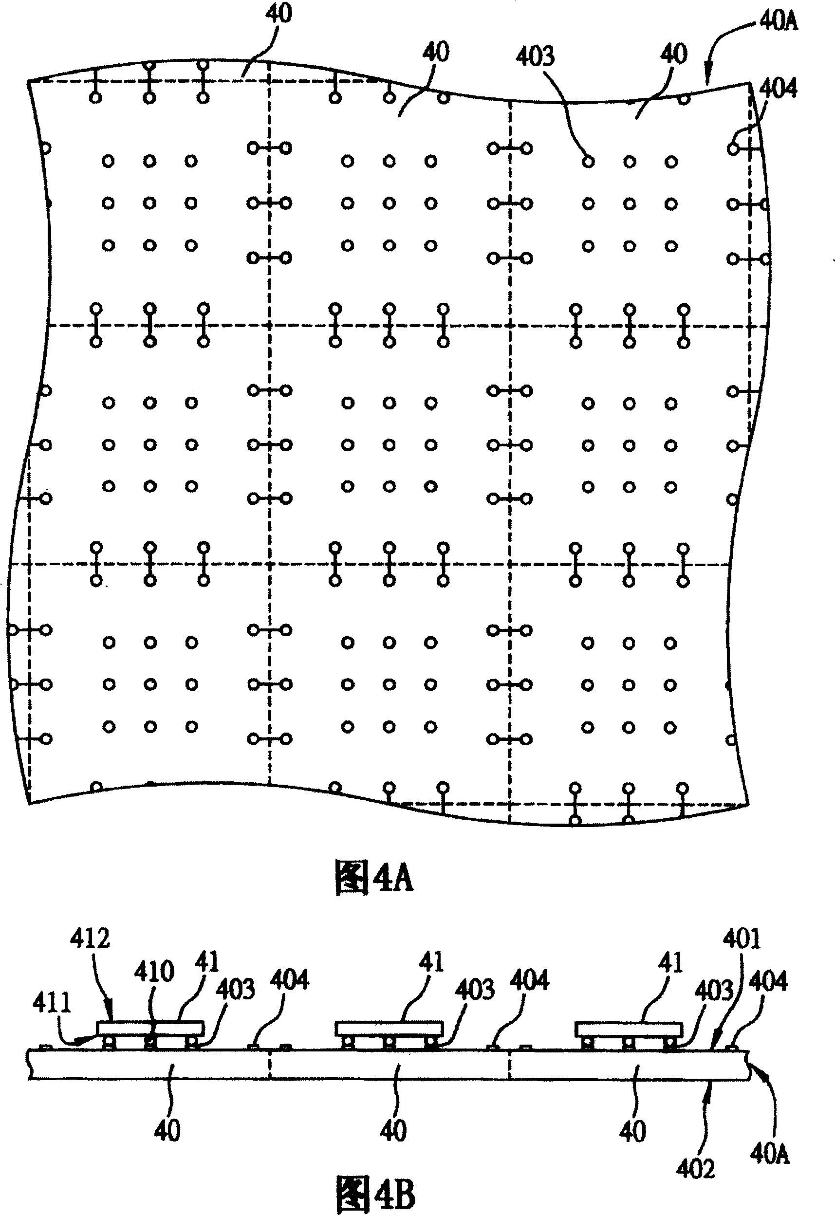
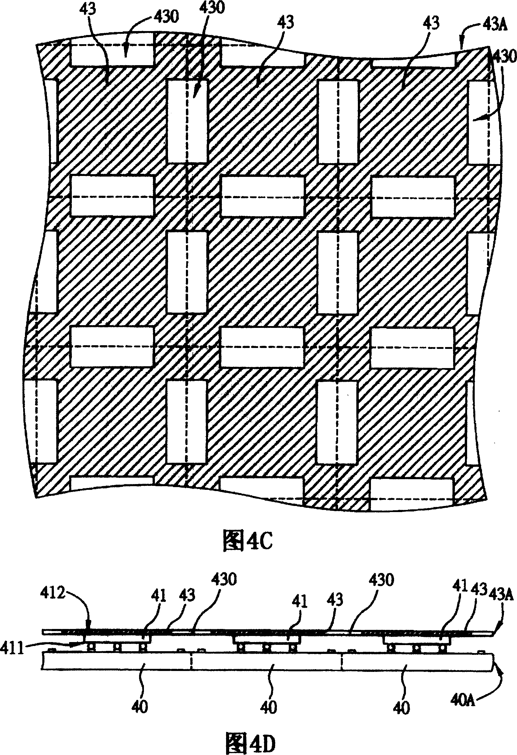
[0036] The semiconductor package of the present invention includes: a chip carrier; a first chip 41 that is connected and electrically connected to the chip carrier; a heat sink 43 formed with a plurality of through openings, connected on the first chip 41 and not Contacting the chip carrier; connecting the second chip 42 on the heat sink, and the second chip 42 is electrically connected to the chip carrier through the wire passing through the opening 430 of the heat sink 43; and formed on the heat sink 43 The encapsulant 45 on the chip carrier covers the first chip 41 , the second chip 42 , the wires and the heat sink 43 . Wherein, the chip carrier is the substrate unit 40.

[0037] Please refer to FIG. 4A to FIG. 4H , which are process diagrams of Embodiment 1 of the stacked chip semiconductor package manufacturing method of the present invention.

[0038] As shown in Figures 4A and 4B, at first, a substrate module sheet 40A is provided, and the substrate module sheet 40A i...

Embodiment 2

[0047] Please refer to FIG. 6 , which is a schematic cross-sectional view of Embodiment 2 of a semiconductor package manufactured by referring to the method for manufacturing a semiconductor package with stacked chips of the present invention. The semiconductor package of the present invention is made by a method similar to that of Example 1. The difference is that in the semiconductor package of Example 2, when the second chip 52 is bonded, the heat dissipation is utilized. The component 53 serves as a ground plane, and electrically connects the second chip 52 to the heat sink 53 through the ground wire 540, so as to improve the electrical function of the semiconductor package. Wherein, in order to improve the connection effect of the grounding wire (gold wire) on the heat sink 53, the connection position of the wire is plated with silver on the heat sink 53 to improve bonding.

Embodiment 3

[0049]Please refer to FIG. 7 , which is a schematic cross-sectional view of Embodiment 3 of the semiconductor package structure manufactured by referring to the semiconductor package method for stacking chips of the present invention. The semiconductor package structure of the present invention is made by a method similar to that of the semiconductor structure of Example 1, the difference is that the chip carrier used in this example is an LGA (LAND GRID ARRAY) substrate 60, so that the first and The second chips 61 , 62 can be electrically connected to external devices via a plurality of metal contacts 60 a arranged on the bottom surface of the LGA substrate 60 .


PUM


Abstract

The semiconductor package consists of a chip carrier, a first chip connected to the chip carrier, multi heat sinks with through opening formed on the package and connected to the first chip and not touching the chip carrier, a second chip attaching to the heat sinks and connected to the chip carrier via the through opening, and a sealing colloid formed on the chip carrier and covering the first chip, second chip, wire and heat sinks. The invention integrates heat sink into semiconductor package to improve efficiency of heat dispersion of semiconductor chip.

Description

technical field [0001] The present invention relates to a semiconductor package with stacked chips and its manufacturing method, in particular to a semiconductor package with integrated heat sink and stacked chips and its manufacturing method. Background technique [0002] With the vigorous development of the electronic industry, electronic products are gradually developing towards multi-functional and high-performance directions to meet the packaging requirements of high integration and miniaturization of semiconductor packages. In order to improve the performance and capacity of a single semiconductor package, in line with the trend of miniaturization, large capacity and high speed of electronic products, most of the existing products present the semiconductor package in the form of a multi-chip module (Multi Chip Module; MCM). This kind of package can reduce the volume of the whole package and improve the electrical function, so it becomes a mainstream of package. It is ...

Claims


Application Information

Patent Timeline
Patent Type & Authority Patents(China)
IPC IPC(8): H01L21/50H01L25/00H01L25/065
CPCH01L24/97H01L2224/16H01L2224/32145H01L2224/48091H01L2224/48227H01L2224/49171H01L2224/73265H01L2924/15311H01L2924/351H01L2924/181H01L2224/97H01L2924/00014H01L2924/00
Inventor 黄建屏
Owner SILICONWARE PRECISION IND CO LTD
Why Eureka
Try Eureka