Electronic components and their manufacture

一种电子零件、制造方法的技术,应用在电子零件及其制造领域,能够解决导电端子盘难对准、ACF价格高、填充树脂注入费功夫等问题

Inactive Publication Date: 2007-10-31
SEIKO EPSON CORP
View PDF3 Cites 0 Cited by
  • Summary
  • Abstract
  • Description
  • Claims
  • Application Information

AI Technical Summary

Problems solved by technology

[0005] For example, in the method of filling a filling resin between an electronic component and a circuit board, it may take a lot of effort to inject the filling resin
[0006] In addition, in the mounting method using ACF, the conductive particles must be very small when the gap between the terminals is small, resulting in a high price of ACF
[0007] In addition, in the method described in Japanese Unexamined Patent Application Publication No. 2003-124259, it may be difficult to align the bump electrodes of the IC chip with the conductive terminal pads on the circuit board.

Method used


Image

  • Electronic components and their manufacture
  • Electronic components and their manufacture
  • Electronic components and their manufacture

Examples


Embodiment Construction

[0053] Hereinafter, embodiments of the present invention will be described with reference to the drawings. In addition, the accompanying drawings in the following description are schematic diagrams of the structures of various embodiments of the present invention, and the shapes and size ratios in the drawings do not represent the actual shapes and sizes of the present invention.

[0054] (first embodiment)

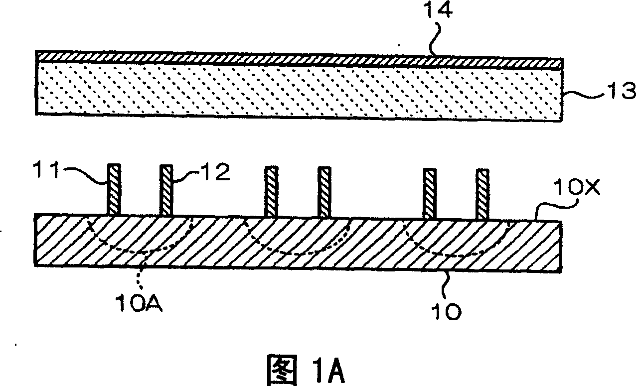
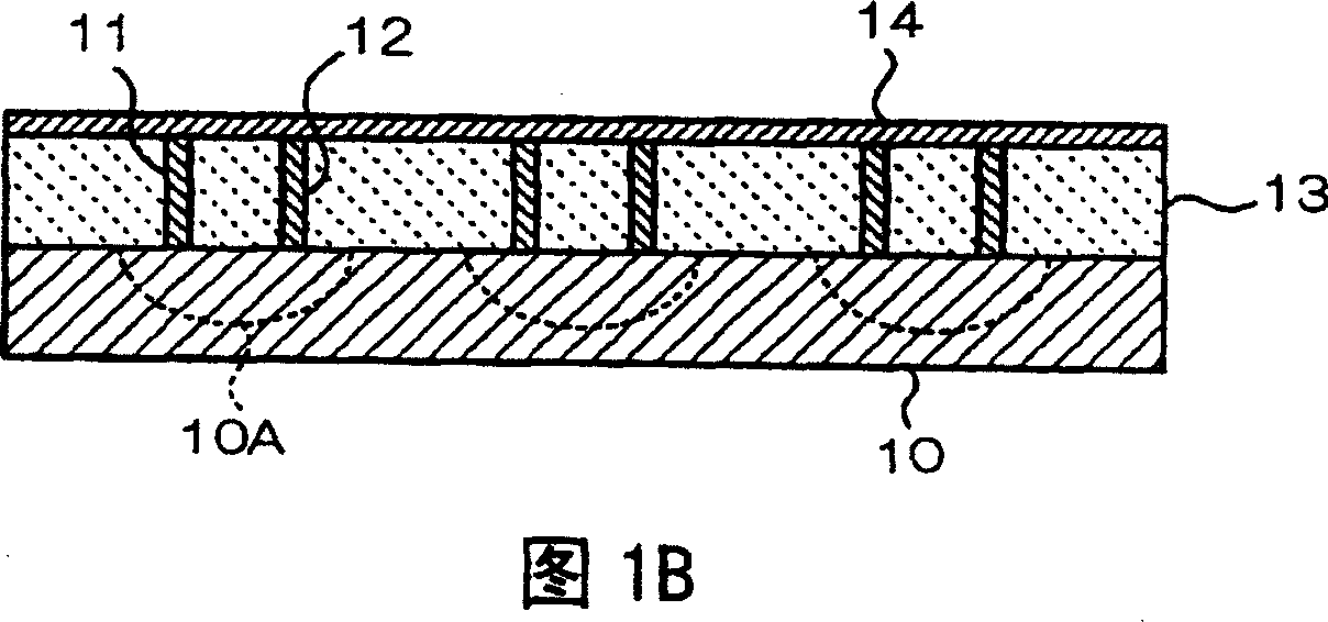
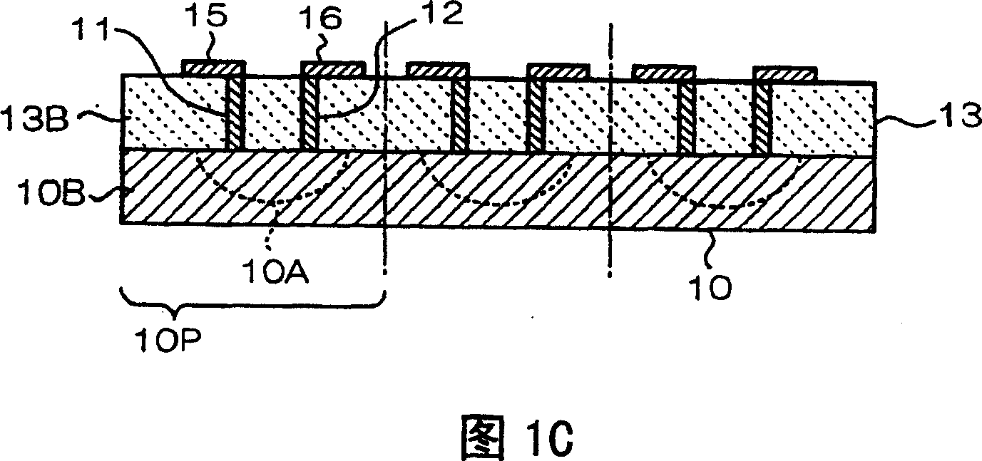
[0055] First, a first embodiment of the present invention will be described with reference to FIGS. 1A to 1C . In this embodiment, as shown in FIG. 1A , a semiconductor substrate 10 in which a plurality of integrated circuits 10A are integrated is prepared. The semiconductor substrate 10 is made of single crystal silicon or a compound semiconductor single crystal, and may be a semiconductor substrate having a predetermined electronic circuit structure as the integrated circuit 10A. Alternatively, the semiconductor substrate 10 may also be a ceramic substrate. The semic...


PUM

PropertyMeasurementUnit
distanceaaaaaaaaaa
heightaaaaaaaaaa

Abstract

A method of manufacturing an electronic component, including: forming a thermoplastic resin layer on a surface of a semiconductor substrate including a plurality of integrated circuits and a bump electrode provided on each of the integrated circuits, to bury the bump electrode; forming a conductive pattern on a surface of the thermoplastic resin layer opposite to the semiconductor substrate, and electrically connecting the conductive pattern to the bump electrode; and dividing the semiconductor substrate in units of the integrated circuits.

Description

technical field [0001] The invention relates to an electronic component and a method for manufacturing the same. Background technique [0002] In general, in various electronic devices, electronic components such as semiconductor ICs are mounted on circuit boards or the like to form part of circuits. There are various methods of mounting electronic components on a circuit board or the like. For example, the most common method is to fill the gap between the electronic component and the circuit substrate with a filling resin to seal it and mount it in a state where the bump electrodes of the electronic component are in contact with the conductive terminal pads on the circuit substrate. [0003] In addition, as a mounting method widely used in manufacture of liquid crystal display devices, etc., electronic components can be mounted using an anisotropic conductive film (ACF; Anisotropic Conductive Film). In this method, electronic components are pressed onto a glass substrate ...

Claims


Application Information

Patent Timeline
Patent Type & Authority Patents(China)
IPC IPC(8): H01L21/00G02F1/13H05K3/32G02F1/1345H01L21/56H01L21/60H01L23/12H01L23/31H01L23/48H05K3/00
CPCH01L2924/09701H01L2924/01027H01L2224/03505H01L2924/01002H01L2924/12044H01L2924/12041H01L21/56H01L2924/01015H01L2924/0105H01L2924/01047H01L2924/01006H01L24/16H01L2924/19041H01L24/11H01L2924/01079H01L2924/14H01L2924/01005H01L23/3114H01L2924/0103H01L2224/13099H01L2924/01013H01L24/03H01L24/12H01L2224/0401H01L2924/01029H01L2924/01033H01L2924/01075H01L2924/15787H01L2924/12042H01L2924/00G02F1/1345
Inventor 斋藤淳
Owner SEIKO EPSON CORP
Why Eureka
Try Eureka