Method for manufacturing semiconductor chip

A manufacturing method and semiconductor technology, applied in semiconductor/solid-state device manufacturing, semiconductor devices, manufacturing tools, etc., can solve problems such as semiconductor chip cracking and broken damage, semiconductor chip damage, and difficulty in re-attaching

Inactive Publication Date: 2007-08-29
SEKISUI CHEM CO LTD +1
View PDF5 Cites 0 Cited by
  • Summary
  • Abstract
  • Description
  • Claims
  • Application Information

AI Technical Summary

Problems solved by technology

[0004] However, when using a dicing device to cut a semiconductor wafer thinned by back grinding, the semiconductor wafer needs to be reattached to the dicing tape after the semiconductor wafer is peeled off from the support plate, so there is a risk of damaging the semiconductor wafer during peeling or pasting.
In particular, it is very difficult to reattach without damage to semiconductor wafers formed very thinly by grinding the thickness of 100 μm or less and 50 μm or less
[0005] In addition, for example, in the invention disclosed in Japanese Patent Application Laid-Open No. 10-284449, grinding and dicing are performed while the surface of the semiconductor wafer is attached to the holding tape, so it is not necessary to re-attach when transferring from grinding to dicing, but After dicing, when the semiconductor chip is peeled off from the dicing tape, there is a risk of damage, deformation, etc., such as cracking and chipping of the semiconductor chip

Method used


Image

  • Method for manufacturing semiconductor chip
  • Method for manufacturing semiconductor chip
  • Method for manufacturing semiconductor chip

Examples


Embodiment Construction

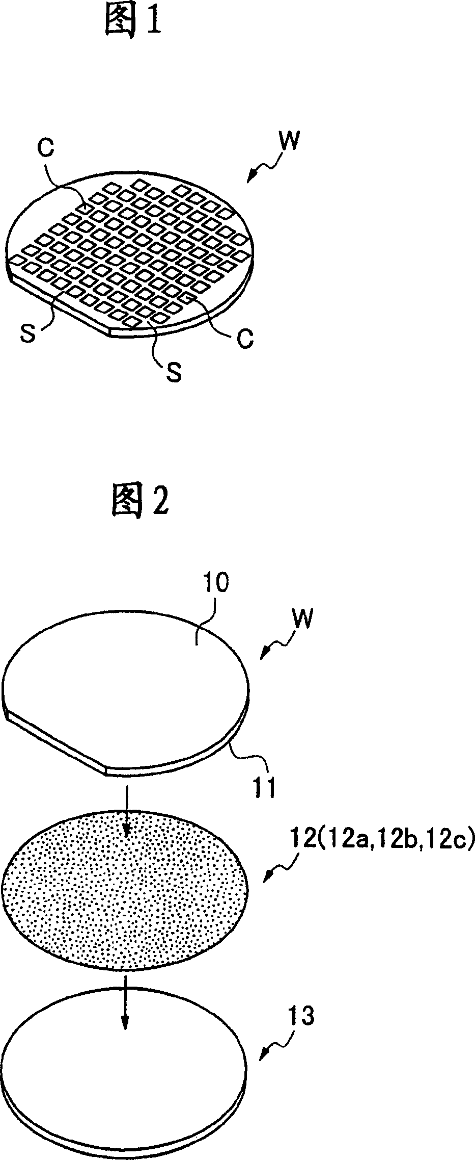
[0024] As a preferred mode for carrying out the present invention, a method for manufacturing individual semiconductor chips C by grinding the back surface of the semiconductor wafer W shown in FIG. 1 and cutting (dicing) the channels S vertically and horizontally will be described below.

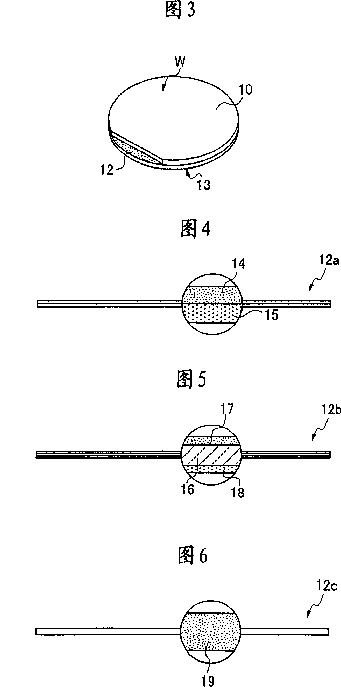
[0025] In the semiconductor wafer W shown in FIG. 1 , circuits are formed on the surface of the regions divided by the channels S. As shown in FIG. As shown in FIG. 2, under the state that the semiconductor wafer W is turned over so that the back surface 10 faces upward, the surface of the semiconductor wafer W is pasted on the support plate 13 through the adhesive sheet 12, and it is integrated as shown in FIG. 3 ( support plate integration process). That is, the surface 11 of the semiconductor wafer W is pasted on the adhesive sheet 12 .

[0026] The adhesive sheet 12 has a property of reducing the adhesive force by excitation, and is, for example, an adhesive sheet containing a gas gene...


PUM


Abstract

A semiconductor wafer (W) where circuits are formed in the area divided by streets is split into semiconductor chips having individual circuits. By interposing an adhesive sheet, whose adhesive force is lowered by stimulation, between the semiconductor wafer (W) and the support plate ( 13 ), the front side of the semiconductor wafer (W) is adhered to the support plate ( 13 ), thereby exposing the rear face ( 10 ) of the semiconductor wafer (W). The rear face ( 10 ) of the semiconductor wafer (W) with the support plate ( 13 ) is ground. After the grinding is finished, the semiconductor wafer (W) held with the rear face ( 10 ) up is diced into semiconductor chips (C). The adhesive sheet is given stimulus to lower the adhesive force and the semiconductor chips (C) are removed from the support plate ( 13 ). The semiconductor wafer and semiconductor chips are always supported by the support plate, avoiding damage and deformation.

Description

technical field [0001] The present invention relates to a method of manufacturing a semiconductor chip for preventing damage, deformation, etc. of the semiconductor wafer and the semiconductor chip during the process of grinding the back surface of the semiconductor wafer and then dicing to form the semiconductor chip. Background technique [0002] As shown in FIG. 14, the back surface of the semiconductor wafer W in which circuits are formed in a plurality of regions C divided by channels S is ground to form a desired thickness, and then the channels S are cut vertically and horizontally to form semiconductors such as ICs and LSIs. chip. [0003] When polishing the back surface, since the surface side is held by the polishing device, a protective tape is usually attached to the surface in order to protect the circuit formed on the surface. In addition, in order to realize the miniaturization and thinning of various electronic devices, when the thickness of the semiconducto...

Claims


Application Information

Patent Timeline
Patent Type & Authority Patents(China)
IPC IPC(8): H01L21/301B24B7/22B24B41/06H01L21/00H01L21/304H01L21/68H01L21/78
CPCH01L21/78B24B41/068H01L21/67092H01L21/67132H01L21/6836H01L21/6835H01L21/304H01L2221/6834H01L2221/68327B24B7/228Y10S438/977
Inventor 福冈正辉畠井宗宏林聪史大山康彦檀上滋北村政彦矢嶋兴一
Owner SEKISUI CHEM CO LTD
Why Eureka
Try Eureka