
Optical device

a technology of optoelectronic devices and optical components, applied in the direction of solid-state devices, electrical devices, photovoltaic energy generation, etc., can solve the problems of further constraints on design, impact cost, and pitaxial defects in conventional, point, thread and dislocation defect types, so as to simplify optical design of structures, reduce angular cones, and high directionality

Active Publication Date: 2018-06-05
UNIV OF SOUTHAMPTON
View PDF10 Cites 1 Cited by
  • Summary
  • Abstract
  • Description
  • Claims
  • Application Information

AI Technical Summary

Benefits of technology

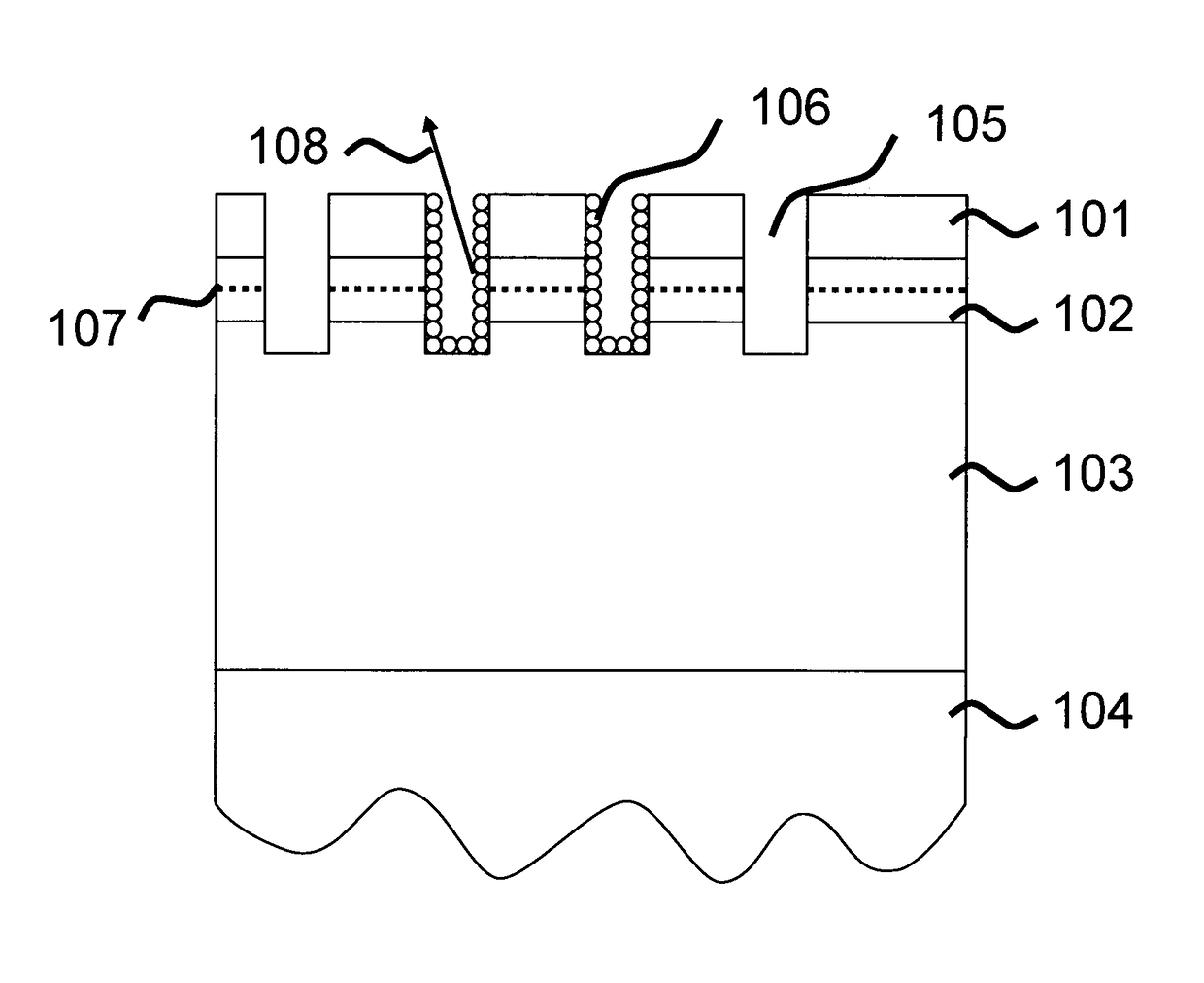
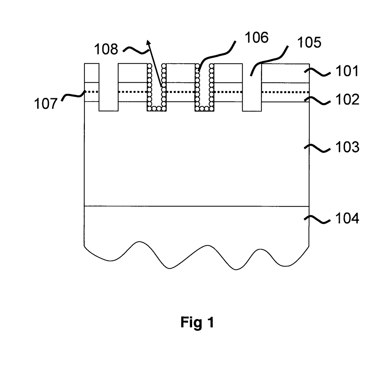
[0049]The present invention relates to device configurations which optimise light extraction or collection per unit surface area via improvement of the efficiency of non-radiative energy transfer, and via an increase in number of carriers (exciton pairs) actively involved in the light emission or collection process. Crucially (and in contrast to prior art) the present invention involves the utilisation of a shaped cavity (or cavities) formed through the structure, which permit optically responsive nanoparticles to be deposited onto the side wall(s) of the cavity such that nanoparticles are disposed around an internal perimeter of the cavity in very close proximity (or contact) to the energy transfer region where the non-radiative energy transfer takes place. As will be described, this approach allows the cavity (or cavities) to be configured for optimal performance in respect of a number of device parameters. Where the cavity, or cavities, contains a single optically responsive particle, the device can operate as a single photon device, either in an emitting mode or in an absorbing (detecting) mode of operation.
[0084]As will be appreciated by those skilled in the art, the present invention provides for significantly improved optoelectronic devices. The use of optically responsive particles permits the light generating / absorbing function to be separated from the electrical driving / generating function, which when combined with the use of innovative shaped cavity structures provides for wide design possibilities and device functionality. Each facet of the device can thus be optimised for the particular application at hand.

Problems solved by technology

Epitaxial defects in conventional LEDs can include point, thread and dislocation defect types.
To reduce defect density the epitaxial layers must be matched in lattice constant to an underlying substrate material which further places constraints on their design and impact cost.
Non-transparent metal contact stacks are then deposited onto this which subsequently mask part of the light emitting area and thus reduce efficiency of the device.
Sapphire (which is well lattice matched to GaN) is a poor heat conductor and so such devices of this design suffer reduced lifetimes, if driven at the very high current densities which are required for general lighting applications.
Additionally, the necessity for a thin optically transparent top current spreading layer places constraints on the achievable contact resistance, and therefore on electrical efficiency of the device.
A key intrinsic problem for conventional LEDs is the issue of poor light extraction efficiency.
Due to the relatively high refractive index of common semiconductor materials combined with the fact that light is generated deep within the epitaxial structure, Fresnel reflection at the semiconductor / air interface causes confinement of a large proportion of the radiated energy.
This factor severely limits the wall plug efficiency for conventional LEDs.
In both cases the positions of the random structures are seeded by epitaxial defect sites, and hence this technique is not compatible or beneficial with very high quality low defect density epitaxy.
Photons incident upon the phosphors are therefore subject to further Fresnel reflection which again severely inhibits the efficiency of photon absorption to the phosphor.
Hence the efficiency of the overall process is still quite low.
In addition it is very difficult to find phosphors with all the correct properties to cover certain colour ranges, and so the wallplug efficiency of phosphor-converted LEDs varies considerably with colour.
There are further lifetime issues associated with differential aging rates for mixtures of phosphors, which results in colour temperature shifts as well as heat related reduction in efficiency.
OLED devices overcome some of the intrinsic loss issues associated with conventional LEDs, but suffer from issues of limited lifetime.
Efficiency is limited by the fact that absorption only occurs efficiently over a limited spectral range for photons with energies above the semiconductor band gap energy.
Excess energy exceeding the band gap energy is also lost as heat for photons with higher than band gap energies.
Fabrication of triple junction solar cells is extremely difficult due to the requirement for precise lattice matching between successive material layers during epitaxial growth procedures.
There are therefore issues associated with differing maximum power handling capabilities for the successive junction regions which reduce maximum attainable efficiency.
An issue for all of the above described PV solar technologies is the reduction of optical loss.
The efficiency of radiative energy transfer in this case is relatively low due to several energy loss steps in the transfer process, i.e. the waveguided leaky mode losses, light scattering from the NQDs, and the reduced efficiency of emission in the blue, absorption and reemission from the NQD layers.
Notwithstanding these developments, a practical issue limiting efficient realisation of both light emitting and light harvesting applications of non radiative energy transfer processes is the requirement to bring the light emitting / collecting particle into close proximity to the heterostructure, while still providing suitable conduction channels to the energy transfer region.
As a consequence, an undesirable tradeoff exists between these requirements.

Method used


Image

  • Optical device
  • Optical device
  • Optical device

Examples


first embodiment

of a Light Harvesting Device Incorporating a p-n Junction

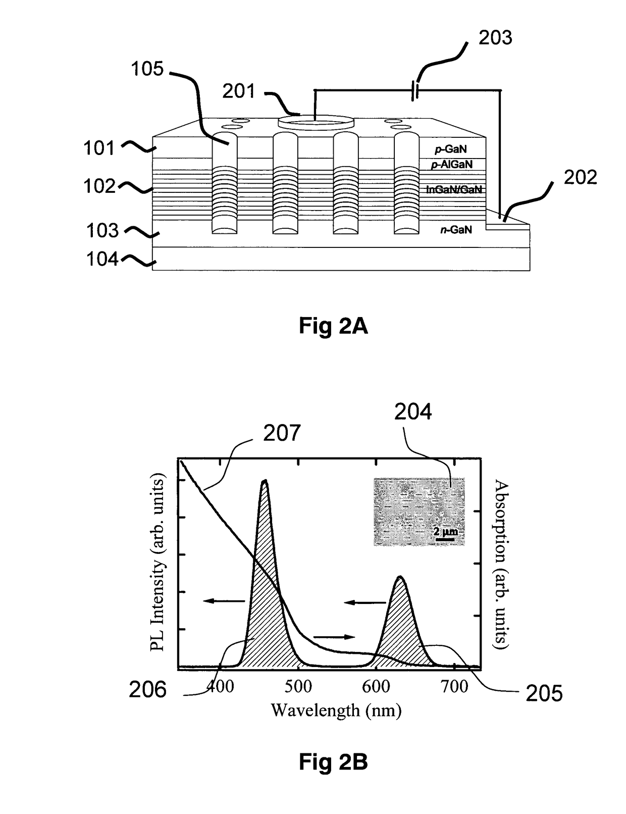
[0168]For purpose of example we now discuss in detail the practical implementation and demonstration of the first embodiment of the present invention as a light harvesting device with reference to the figures whereby the composite enclosing structure incorporates a single p-i-n junction as the energy transfer region in a configuration, leading to strong enhancement of the measured photocurrent. The excited state energy of the deposited NCs is efficiently transferred to a patterned bulk heterostructure by means of nonradiative energy transfer. Electron-hole pairs transferred to the heterostructure are subsequently separated by the built-in electric field and are collected by the electrodes resulting in electrical current.

[0169]The semiconductor bulk heterostructure used in this example offers higher carrier transport than the QW heterostructure in the previous example. In this configuration, wide absorption range and high oscil...

second embodiment

of the Invention

[0178]In a second embodiment of the invention (where the refractive index of the enclosing structure shown in FIG. 1 (101-103) is larger than that of the shaped structures shown in FIG. 1 (105), a large proportion of emitted light becomes reflected back from the side walls of the shaped structures, due to Fresnel reflection at the low to high refractive index boundary at the surface interface, such that each shaped structure acts predominantly as a reflective cavity for light emitted from (or collected by) the light emitting (or light absorbing) particle providing further beneficial effects as will now be described.

[0179]FIG. 13 shows in more detail the process of light emission from the optically responsive particle under such circumstances. A light ray (1301) emitted from a optically responsive particle (106) placed in close proximity to the energy transfer region (107), radiating towards the direction of the proximal heterostructure, becomes predominantly reflecte...

third embodiment

of the Invention

[0196]In a third embodiment of the invention, the enclosing structure incorporates a number of energy transfer regions perforated by a shaped structure (FIG. 21) such that more than one energy transfer region (2101) participates in the non-radiative energy transfer process to or from the colloidal nanoparticles. In this embodiment of the invention emission power (brightness), or collection efficiency, scales with number of perforated quantum wells.


PUM


Abstract

An improved optoelectronic device is described, which employs optically responsive nanoparticles and utilises a non-radiative energy transfer mechanism. The nanoparticles are disposed on the sidewalls of one or more cavities, which extend from the surface of the device through the electronic structure and penetrate the energy transfer region. The nanoparticles are located in close spatial proximity to an energy transfer region, whereby energy is transferred non-radiatively to or from the electronic structure through non-contact dipole-dipole interaction. According to the mode of operation, the device can absorb light energy received from the device surface via the cavity and then transfer this non-radiatively or can transfer energy non-radiatively and then emit light energy towards the surface of the device via the cavity. As such, the deice finds application in light emitting devices, photovoltaic (solar) cells, displays, photodetectors, lasers and single photon devices.

Description

CROSS REFERENCE TO RELATED APPLICATION[0001]The present application is the U.S. national stage application of International Application PCT / GB2010 / 000273, filed Feb. 16, 2010, which international application was published on Aug. 19, 2010, as International Publication WO2010 / 092362. The International Application claims priority of British Patent Application 0902569.3, filed Feb. 16, 2009.FIELD OF THE INVENTION[0002]The present invention relates to improved optoelectronic devices which employ optically responsive nanoparticles and utilise a non-radiative energy transfer mechanism, and particularly to practical device configurations for improving the efficiency of operation. Such devices include light emitting devices, photovoltaic (solar) cells, displays, photodetectors, lasers and single photon devices.BACKGROUND TO THE INVENTION[0003]In view of raised global awareness of the depletion of non-renewable energy sources and the associated impact on the environment there is intense inte...

Claims


Application Information

Patent Timeline
Patent Type & Authority Patents(United States)
IPC IPC(8): H01L31/0352H01L27/146H01L31/055H01L31/0232H01L33/20H01L33/50H01L33/00H01L33/08
CPCH01L31/02322H01L27/14603H01L31/0352H01L31/035281H01L33/20H01L33/505H01L31/055Y02E10/52H01L33/0004H01L33/08
Inventor CHARLTON, MARTIN DAVID BRIANLAGOUDAKIS, PAVLOSCHANYAWADEE, SOONTORN
Owner UNIV OF SOUTHAMPTON
Learn More