Devices and methods for oligonucleic acid library synthesis
a technology of oligonucleic acid and library, applied in the field of devices and methods for oligonucleic acid library synthesis, can solve the problems of scalability, automation, speed, accuracy, cost, etc., and achieve the effects of improving efficiency, speed, accuracy, and cos
- Summary
- Abstract
- Description
- Claims
- Application Information
AI Technical Summary
Benefits of technology
Problems solved by technology
Method used
Image
Examples
example 1
lization of a Substrate Surface
[0180]A substrate was functionalized to support the attachment and synthesis of a library of oligonucleic acids. The substrate surface was first wet cleaned using a piranha solution comprising 90% H2SO4 and 10% H2O2 for 20 minutes. The substrate was rinsed in several beakers with DI water, held under a DI water gooseneck faucet for 5 min, and dried with N2. The substrate was subsequently soaked in NH4OH (1:100; 3 mL:300 mL) for 5 min, rinsed with DI water using a handgun, soaked in three successive beakers with DI water for 1 min each, and then rinsed again with DI water using the handgun. The substrate was then plasma cleaned by exposing the substrate surface to O2. A SAMCO PC-300 instrument was used to plasma etch O2 at 250 watts for 1 min in downstream mode.
[0181]The cleaned substrate surface was actively functionalized with a solution comprising N-(3-triethoxysilylpropyl)-4-hydroxybutyramide using a YES-1224P vapor deposition oven system with the f...
example 2
on of Substrates Having Distinct Loci Configurations
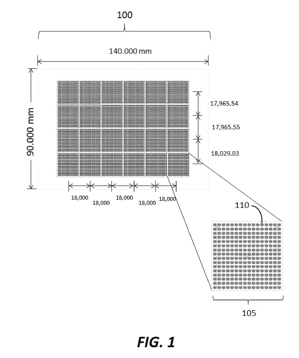
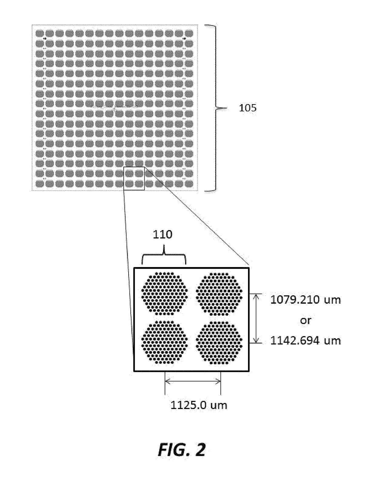
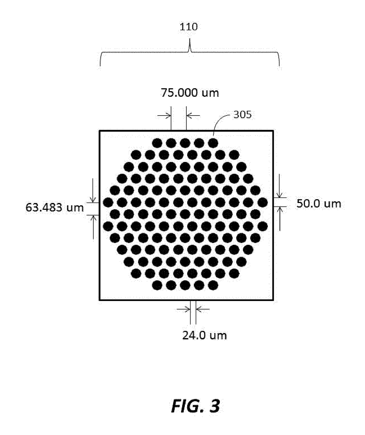
[0184]Substrates were manufactured to comprise a plurality of clusters each comprising a plurality of distinct loci configured to provide structural support for oligonucleic acid synthesis. Substrate starting material was a 200 mm standard, double-sided polished silicon wafer having a 725 um thickness. Substrates were processed by a method comprising thermal oxidation at 1000 Å, photolithography using a Karl Suss MA6 mask aligner to generate fiducial structures; oxide etching down to the silicon; and resist stripping. Prepared substrates have 6,144 clusters, with each cluster having 121 reaction sites or loci for oligonucleic acid synthesis. The clusters are organized into 24 sub-fields, which each comprise a 16×16 array of clusters. A schematic of a substrate produced is shown in FIGS. 1-3. As shown in FIG. 1, the substrate has a dimension of 140.000 mm by 90.000 mm. As shown in FIG. 2, the vertical distance between the centers of...
example 3
ion of Microchannel Surface Area
[0185]Substrates manufactured in this example were processed to generate three-dimensional loci having shapes configured to increase surface area to volume. Examples of locus shapes prepared using the methods described in this example are shown in FIG. 5. A Silicon on Insulator (SOI) silicon wafer (sub-field size of 32.00×32.00 mm) was oxidized, and the device side processed by photolithography, deep RIE and photoresist stripping. The handle side of the substrate was processed by photolithography, deep RIE, photoresist stripping, and etching by removal of oxide layer (BOX etch). The processed substrate has a plurality of wells or holes within the handle layer, each having a width of 1.150 mm, wherein each channel has a plurality of microchannels having shapes that allow for an increase in surface area to volume. The smallest etch size for a feature of a shape of a microchannel within a substrate prepared in this example was 5 um. The distance between ...
PUM
| Property | Measurement | Unit |
|---|---|---|
| surface area | aaaaa | aaaaa |
| surface area | aaaaa | aaaaa |
| width | aaaaa | aaaaa |
Abstract
Description
Claims
Application Information
 - R&D
- Intellectual Property
- Life Sciences
- Materials
- Tech Scout
- Unparalleled Data Quality
- Higher Quality Content
- 60% Fewer Hallucinations
Browse by: Latest US Patents, China's latest patents, Technical Efficacy Thesaurus, Application Domain, Technology Topic, Popular Technical Reports.
© 2025 PatSnap. All rights reserved.Legal|Privacy policy|Modern Slavery Act Transparency Statement|Sitemap|About US| Contact US: help@patsnap.com


