Method and apparatus for calculating delay timing values for an integrated circuit design

a technology of delay timing and integrated circuit, which is applied in the direction of instruments, computing, electric digital data processing, etc., can solve the problems of performance degradation of the mosfet device, extra cost in terms of additional area, power and design effort across the entire ic devi

Inactive Publication Date: 2018-05-22
NXP USA INC
View PDF8 Cites 0 Cited by
  • Summary
  • Abstract
  • Description
  • Claims
  • Application Information

AI Technical Summary

Problems solved by technology

N / PBTI stress can cause key reliability issues in MOSFET devices, and manifests as an increase in the threshold voltage (Vth) and consequently a decrease in the drain current and transconductance of the MOSFET device, which results in performance degradation of the MOSFET device.
However, a problem with this conventional approach is that it introduces extra costs in terms of additional area, power and design effort across the entire IC device, including for those parts of the IC device that do not suffer from significant NBTI / PBTI stress, and thus which do not require such generous additional margins.

Method used


Image

  • Method and apparatus for calculating delay timing values for an integrated circuit design
  • Method and apparatus for calculating delay timing values for an integrated circuit design
  • Method and apparatus for calculating delay timing values for an integrated circuit design

Examples


Embodiment Construction

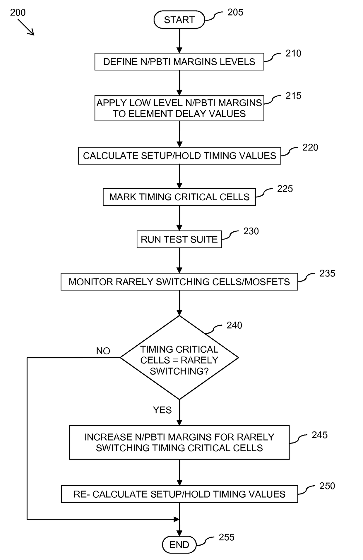
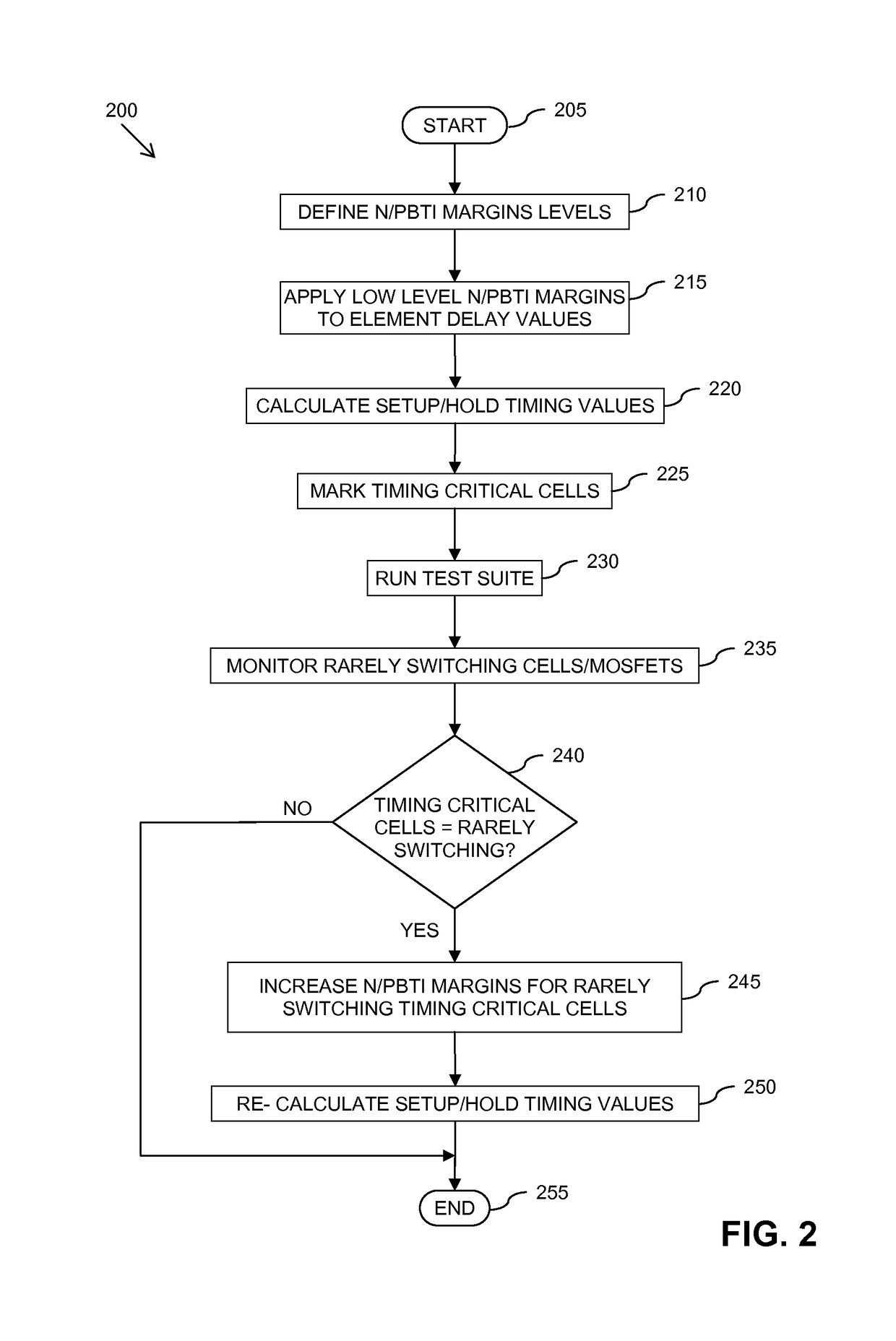
[0011]The present invention will now be described with reference to the accompanying drawings in which examples of a method and apparatus for calculating delay timing values for at least a part of an integrated circuit (IC) design are described and illustrated. However, it will be appreciated that the present invention is not limited to the specific examples illustrated and described herein. Furthermore, because the illustrated embodiments of the present invention may for the most part, be implemented using electronic components and circuits known to those skilled in the art, details will not be explained in any greater extent than that considered necessary as illustrated below, for the understanding and appreciation of the underlying concepts of the present invention and in order not to obfuscate or distract from the teachings of the present invention.

[0012]In accordance with some examples, there is provided a method and apparatus for calculating delay timing values for at least a ...


PUM


Abstract

A method and apparatus for calculating delay timing values for at least a part of an integrated circuit design. The method comprises applying a first Negative / Positive Bias Temperature Instability compensation margin to delay values for elements within the at least part of the IC design, identifying at least one lower-rate switching element within the at least part of the IC design, and applying at least one further, increased N / PBTI compensation margin to the delay value(s) for the at least one identified lower-rate switching element.

Description

FIELD OF THE INVENTION[0001]This invention relates to a method and apparatus for calculating delay timing values for at least a part of an integrated circuit design.BACKGROUND OF THE INVENTION[0002]In the field of modern VLSI (Very Large Scale Integration) integrated circuit (IC) devices, Metal Oxide Semiconductor Field Effect Transistor (MOSFET) devices often have rarely switching periods such as during low power modes, or are simply rarely switching devices, for example within control logic etc. During such periods of non- (or infrequent) switching, a MOSFET device is subjected to a constant bias voltage, which can result in the PMOSFET or NMOSFET device experiencing respectively Negative Bias Temperature Instability (NBTI) or Positive Bias Temperature Instability (PBTI) stress. N / PBTI stress can cause key reliability issues in MOSFET devices, and manifests as an increase in the threshold voltage (Vth) and consequently a decrease in the drain current and transconductance of the MO...

Claims


Application Information

Patent Timeline
Patent Type & Authority Patents(United States)
IPC IPC(8): G06F17/50
CPCG06F17/5031G06F17/5081G06F2217/84G06F30/3312G06F2119/12G06F30/398
Inventor SOFER, SERGEYBERKOVITZ, ASHERPRIEL, MICHAEL
Owner NXP USA INC
Why Eureka
Try Eureka