OLED display panel having opening zone for exposing sub-pixel sub-regions, and method for manufacturing the same
a technology of light-emitting diodes and display panels, which is applied in the field of display panels, can solve the problems of shortening the life of the oled, affecting the efficiency of the oled, and affecting the efficiency of the oled
- Summary
- Abstract
- Description
- Claims
- Application Information
AI Technical Summary
Benefits of technology
Problems solved by technology
Method used
Image
Examples
fourth embodiment
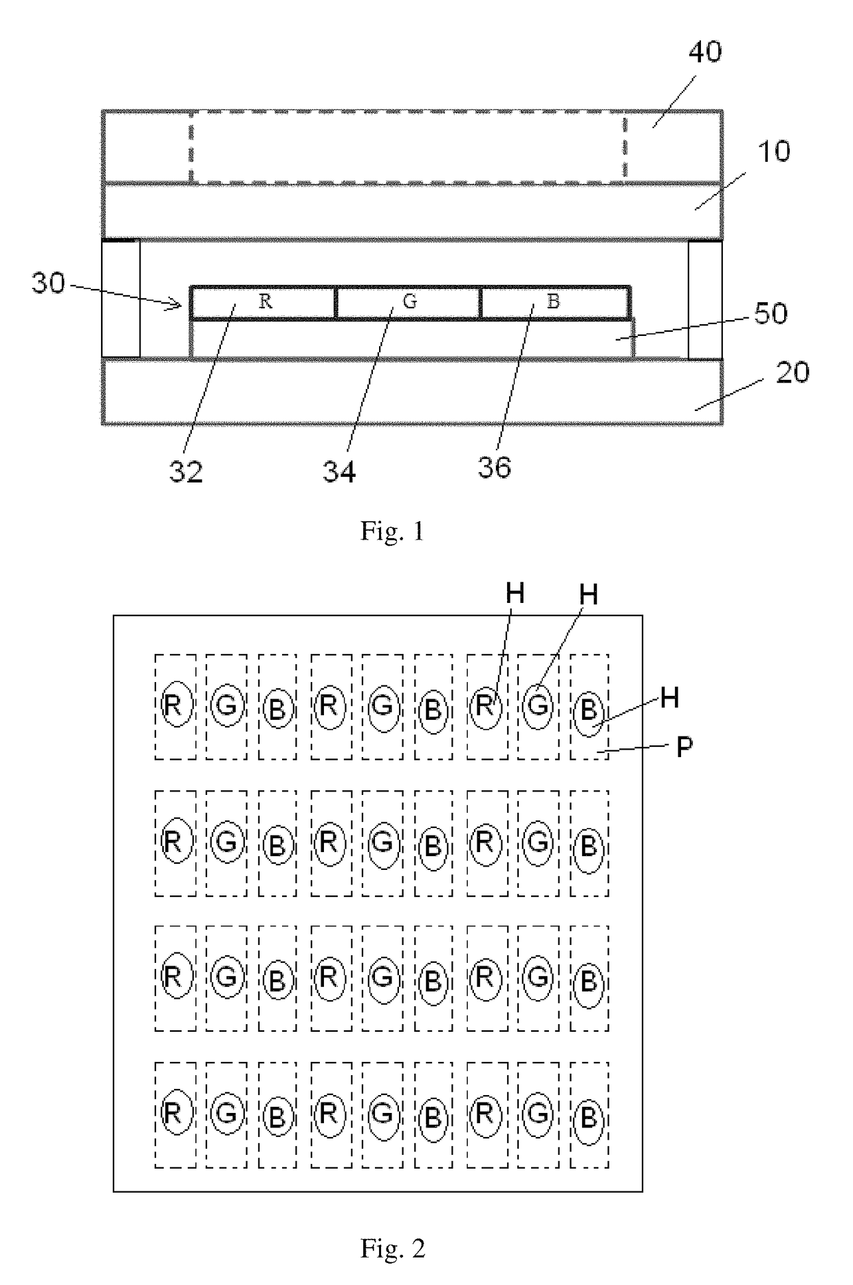
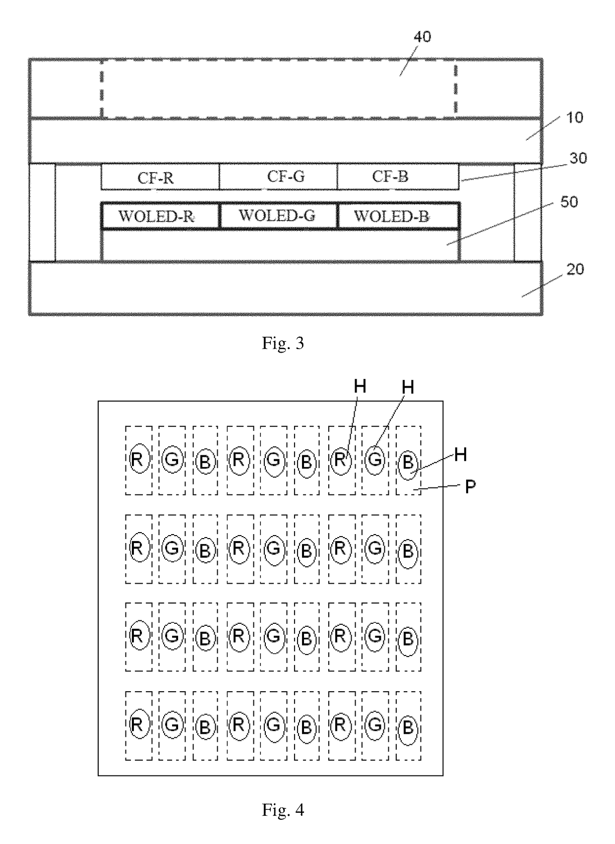
[0050]FIG. 7 is a schematic view showing a structure of an OLED display panel according to a fourth exemplary embodiment of the present invention. FIG. 8 is a top view showing a part of the OLED display panel of FIG. 7. In the fourth embodiment, areas of the circularly polarizing plate where blue sub-pixels B are projected are completely removed. In FIG. 8, solid line boxes denote areas of the circularly polarizing plate corresponding to the blue sub-pixels B are completely removed to expose the sub-pixel sub-regions. As a result, the blue sub-pixels B have 2.5 times increase in efficiency, and power consumption and the current of the whole display panel are decreased by 26%.
fifth embodiment
[0051]FIG. 9 is a schematic view showing a structure of an OLED display panel according to a fifth exemplary embodiment of the present invention. FIG. 10 is a top view showing a part of the OLED display panel of FIG. 9. In the fifth embodiment, areas of the circularly polarizing plate where green sub-pixels G are projected are completely removed. In FIG. 10, solid line boxes denote areas of the circularly polarizing plate corresponding to the green sub-pixels G are completely removed to expose the sub-pixel sub-regions. As a result, the green sub-pixels G have 2.5 times increase in efficiency, and power consumption and the current of the whole display panel are decreased by 13%.
[0052]Although it is not shown, for the structures of the OLED display panels of FIG. 7 and FIG. 9, for example, areas of the circularly polarizing plate where blue sub-pixels B and red sub-pixels R are projected may be completely removed. As a result, the blue sub-pixels B and red sub-pixels R have 2.5 times...
sixth embodiment
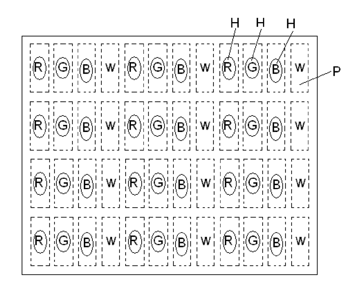
[0055]In the sixth embodiment, areas of the circularly polarizing plate where blue sub-pixels B are projected are completely removed. In FIG. 12, solid line boxes denote areas of the circularly polarizing plate corresponding to the blue sub-pixels B are completely removed to expose the sub-pixel sub-regions. As a result, the blue sub-pixels have 2.5 times increase in efficiency, and power consumption and the current of the whole display panel are decreased by 20%.
[0056]Although it is not shown, for the structure of the OLED display panel of FIG. 11, for example, areas of the circularly polarizing plate where green sub-pixels G are projected may be completely removed. As a result, the green sub-pixels G have 2.5 times increase in efficiency, and power consumption and the current of the whole display panel are decreased by 10%.
[0057]Although it is not shown, for the structure of the OLED display panel of FIG. 11, for example, areas of the circularly polarizing plate where blue sub-pix...
PUM
 Abstract
Description
Claims
Application Information
 - R&D
- Intellectual Property
- Life Sciences
- Materials
- Tech Scout
- Unparalleled Data Quality
- Higher Quality Content
- 60% Fewer Hallucinations
Browse by: Latest US Patents, China's latest patents, Technical Efficacy Thesaurus, Application Domain, Technology Topic, Popular Technical Reports.
© 2025 PatSnap. All rights reserved.Legal|Privacy policy|Modern Slavery Act Transparency Statement|Sitemap|About US| Contact US: help@patsnap.com


