
Grouping memory cells into sub-blocks for program speed uniformity

a memory cell and program speed technology, applied in the field of memory device operation, can solve the problems of variable challenges in the operation of such memory devices

Active Publication Date: 2018-05-01
SANDISK TECH LLC
View PDF11 Cites 16 Cited by
  • Summary
  • Abstract
  • Description
  • Claims
  • Application Information

AI Technical Summary

Benefits of technology

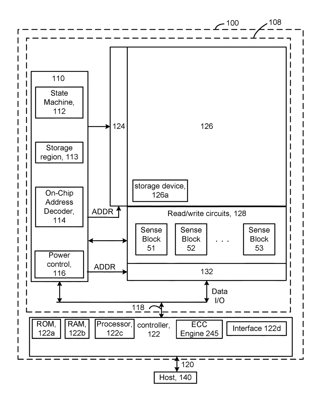
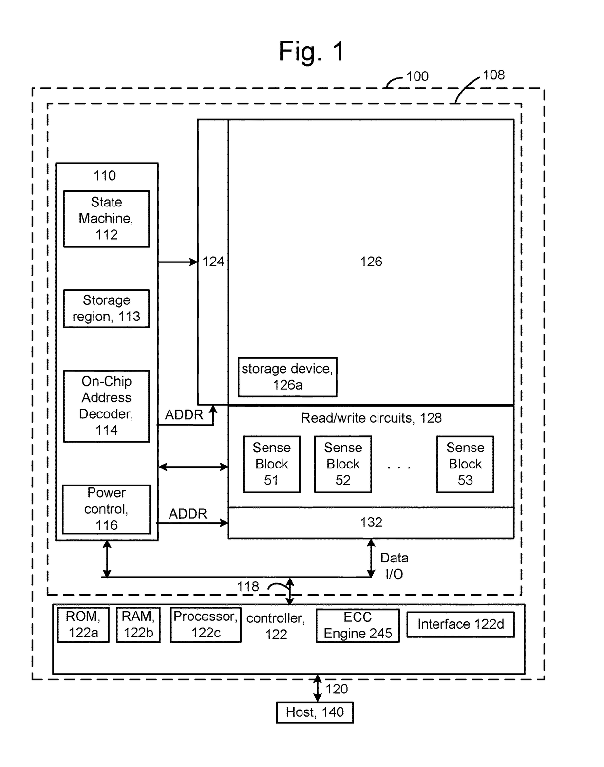
The present technology relates to the operation of memory devices, particularly semiconductor memory devices. The patent text describes various challenges in operating such memory devices and proposes various solutions. The technical effects of the patent text include improving the programming speed of memory cells, reducing the programming time of memory cells, and increasing the reliability of memory cells. The patent text also describes various configurations and arrangements of memory cells in a memory device, including a 3D configuration and a 2D configuration. Overall, the patent text aims to improve the performance and reliability of memory devices by addressing the challenges in their operation.

Problems solved by technology

However, various challenges are presented in operating such memory devices.

Method used


Image

  • Grouping memory cells into sub-blocks for program speed uniformity
  • Grouping memory cells into sub-blocks for program speed uniformity
  • Grouping memory cells into sub-blocks for program speed uniformity

Examples


Embodiment Construction

[0031]Techniques are provided for programming memory cells in a memory device such as a 3D stacked non-volatile memory device with improved program speed uniformity. A corresponding memory device is also provided.

[0032]In some memory devices, memory cells are joined to one another such as in NAND strings in a block or sub-block. Each NAND string comprises a number of memory cells connected in series between one or more drain-side SG transistors (SGD transistors), on a drain-side of the NAND string which is connected to a bit line, and one or more source-side SG transistors (SGS transistors), on a source-side of the NAND string which is connected to a source line. Further, the memory cells can be arranged with a common control gate line (e.g., word line) which acts a control gate. A set of word lines extends from the source side of a block to the drain side of a block. Memory cells can be connected in other types of strings and in other ways as well.

[0033]In a 3D memory structure, th...


PUM


Abstract

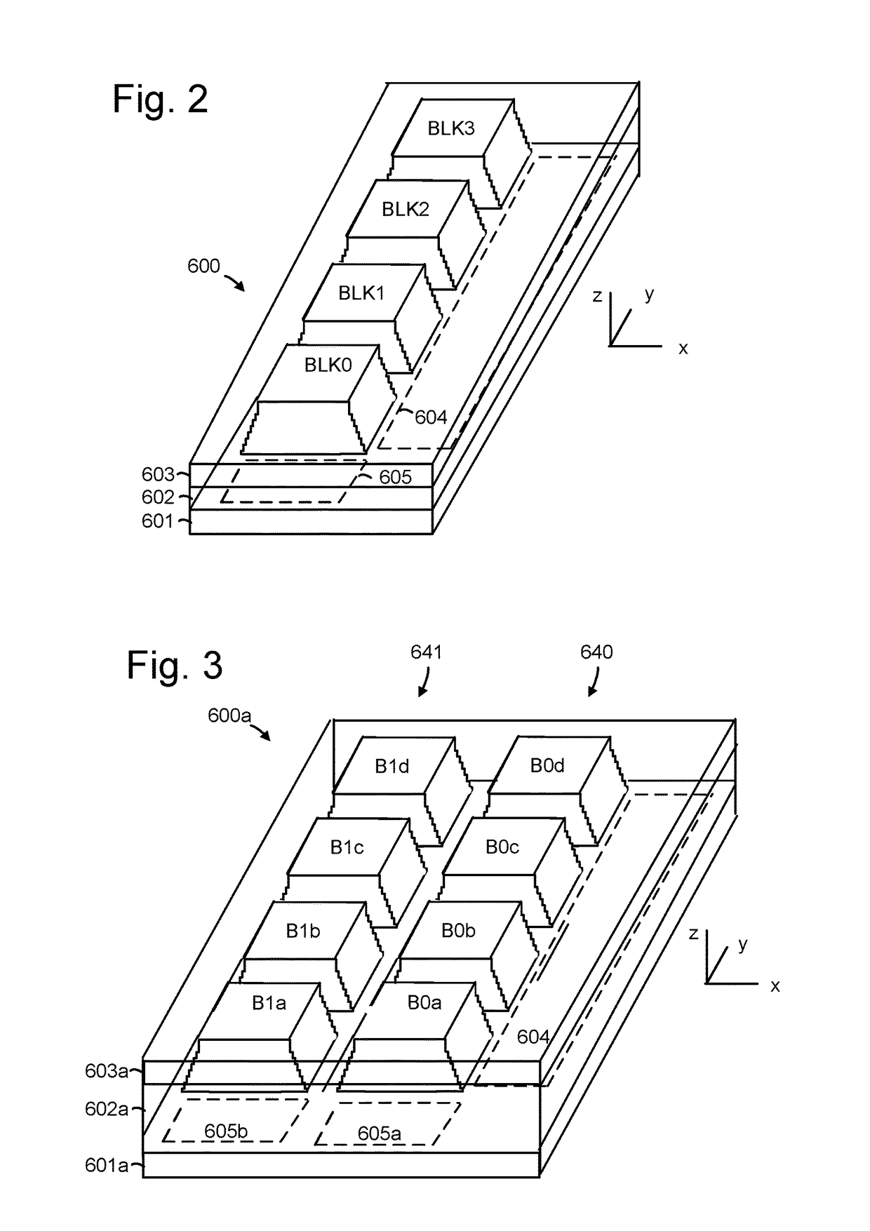
A three-dimensional stacked memory device is configured to provide uniform programming speeds of different sets of memory strings formed in memory holes. In a process for removing sacrificial material from word line layers, a block oxide layer in the memory holes is etched away relatively more when the memory hole is relatively closer to an edge of the word line layers where an etchant is introduced. A thinner block oxide layer is associated with a faster programming speed. To compensate, memory strings at the edges of the word line layers are programmed together, separate from the programming of interior memory strings. A program operation can use a higher initial program voltage for programming the interior memory strings compared to the edge memory strings.

Description

BACKGROUND[0001]The present technology relates to the operation of memory devices.[0002]Semiconductor memory devices have become more popular for use in various electronic devices. For example, non-volatile semiconductor memory is used in cellular telephones, digital cameras, personal digital assistants, mobile computing devices, non-mobile computing devices and other devices.[0003]A charge-storing material such as a floating gate or a charge-trapping material can be used in such memory devices to store a charge which represents a data state. A charge-trapping material can be arranged vertically in a three-dimensional (3D) stacked memory structure, or horizontally in a two-dimensional (2D) memory structure. One example of a 3D memory structure is the Bit Cost Scalable (BiCS) architecture which comprises a stack of alternating conductive and dielectric layers.[0004]A memory device includes memory cells which may be arranged in strings, for instance, where select gate transistors are ...

Claims


Application Information

Patent Timeline
Patent Type & Authority Patents(United States)
IPC IPC(8): G11C16/34G11C16/04G11C16/28G11C16/10
CPCG11C16/3427G11C16/0483G11C16/10G11C16/28G11C16/3459
Inventor ZHANG, ZHENGYIDONG, YINGDAKAI, JAMESALSMEIER, JOHANN
Owner SANDISK TECH LLC
Learn More