Pad structure and manufacturing method thereof
a technology of pad structure and manufacturing method, which is applied in the direction of semiconductor devices, semiconductor/solid-state device details, electrical apparatus, etc., can solve the problems of over-etching of pad at the top of the stacked structure, electrical failure of components, and increase the difficulty of interconnection in the vertical memory device, so as to prevent electrical failures
- Summary
- Abstract
- Description
- Claims
- Application Information
AI Technical Summary
Benefits of technology
Problems solved by technology
Method used
Image
Examples
first embodiment
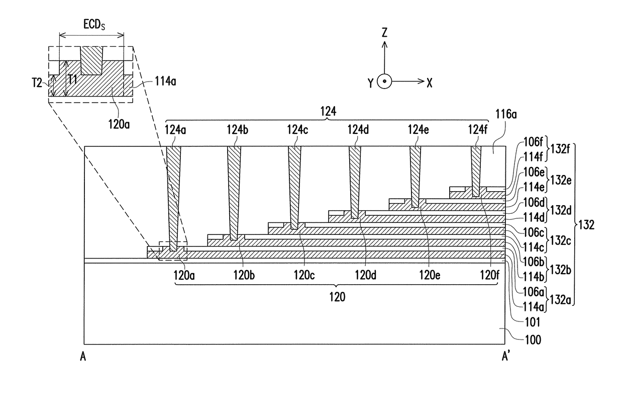
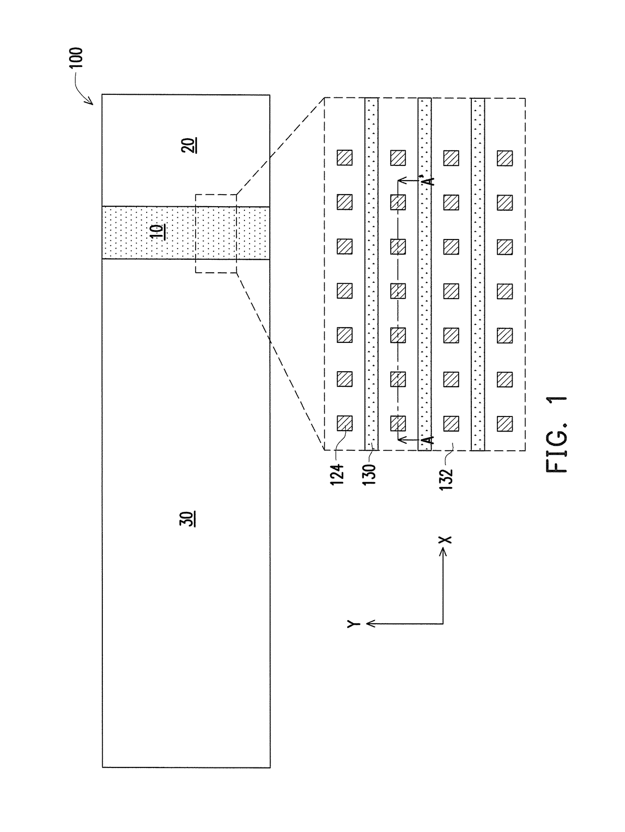
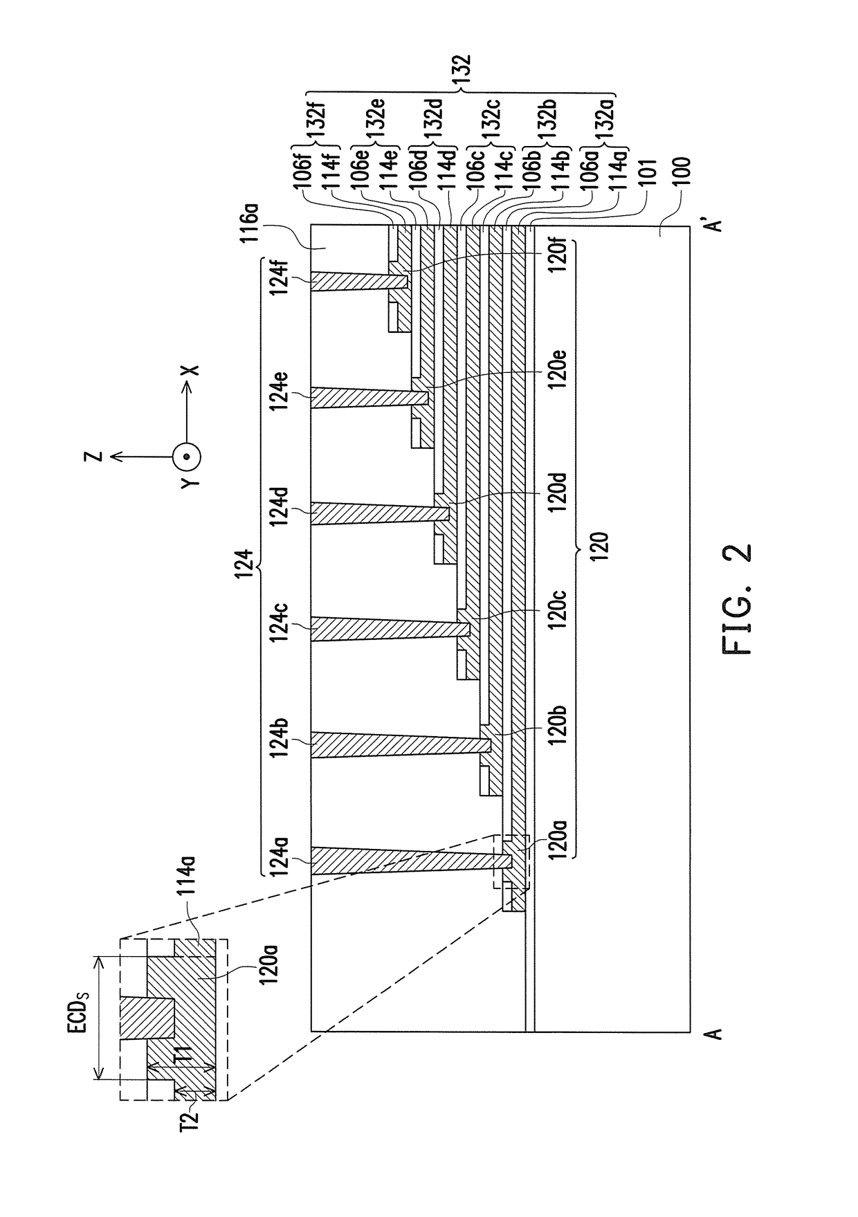
[0065]Please refer to FIG. 4A, FIG. 4B, FIG. 5A, and FIG. 5B. In the first embodiment, the pads 120 and the corresponding contact openings 122 have the square shape. According to an embodiment of the invention, the width ECDs of the pads 120 is greater than the sum of the width ECDc of the contact openings 122 and two specification values S (i.e., ECDs>ECDc+2S). The so-called specification value S refers to an overlay specification value or an overlay tolerance value and is determined by the exposure machine that is applied to perform the manufacturing process of the contact openings. For instance, when the exposure machine applied to perform the manufacturing process of the contact openings is a 193 nm-ArF excimer laser stepper (manufactured by ASML, model 1450H), the specification value S may be in a range of 10 nm to 20 nm, for instance. It should be noted that the pads 120 are the square shape, but the pads 120 eventually formed may be circular shape.
second embodiment
[0066]Please refer to FIG. 6A, FIG. 6B, FIG. 7A, and FIG. 7B. In the second embodiment, the pads 220 have the rectangular shape, and the corresponding contact openings 122 have the square shape. According to an embodiment of the invention, the width ECDs of the pads 220 is greater than the sum of the width ECDc of the contact openings 122 and two specification values S (i.e., ECDs>ECDc+2S).
third embodiment
[0067]Please refer to FIG. 8A, FIG. 8B, FIG. 9A, and FIG. 9B. In the third embodiment, the pads 320 have the bar shape, and the corresponding contact openings 122 have the square shape. The bar-shaped pads 320 are arranged in the X direction and extend along the Y direction. According to an embodiment of the invention, the width ECDs of the pads 320 is greater than the sum of the width ECDc of the contact openings 122 and two specification values S (i.e., ECDs>ECDc+2S).
[0068]To sum up, according to an embodiment of the invention, plural openings may be formed in the topmost material pair of the stacked structure. The stacked structure is patterned to form the stair step structure, and the openings are transferred and formed in each stair step of the stair step structure. The openings are then filled with a conductive material to form the pads. Compared to the conventional pads, the pads provided herein have larger thickness, so as to prevent electrical failures caused by over-etchin...
PUM
 Abstract
Description
Claims
Application Information
 - R&D
- Intellectual Property
- Life Sciences
- Materials
- Tech Scout
- Unparalleled Data Quality
- Higher Quality Content
- 60% Fewer Hallucinations
Browse by: Latest US Patents, China's latest patents, Technical Efficacy Thesaurus, Application Domain, Technology Topic, Popular Technical Reports.
© 2025 PatSnap. All rights reserved.Legal|Privacy policy|Modern Slavery Act Transparency Statement|Sitemap|About US| Contact US: help@patsnap.com


