Wiring structure and printed wiring substrate of wiring structure
a wiring structure and substrate technology, applied in the direction of cross-talk/noise/interference reduction, electrical apparatus construction details, printed circuit non-printed electric components association, etc., can solve the problems of increasing cross-talk noise, difficult to dispose of wirings in a small wiring substrate, and generating cross-talk noise, so as to reduce the cross-talk noise between the wiring patterns and reduce the capacitive coupling and inductive coupling
- Summary
- Abstract
- Description
- Claims
- Application Information
AI Technical Summary
Benefits of technology
Problems solved by technology
Method used
Image
Examples
first embodiment
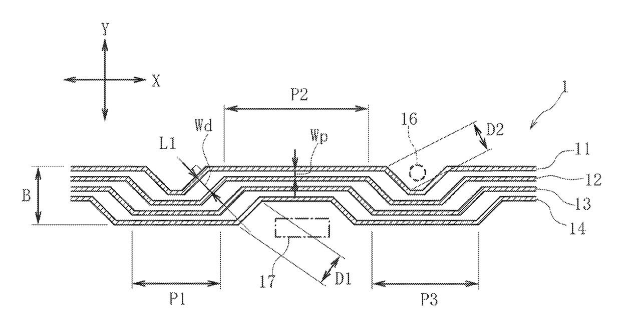
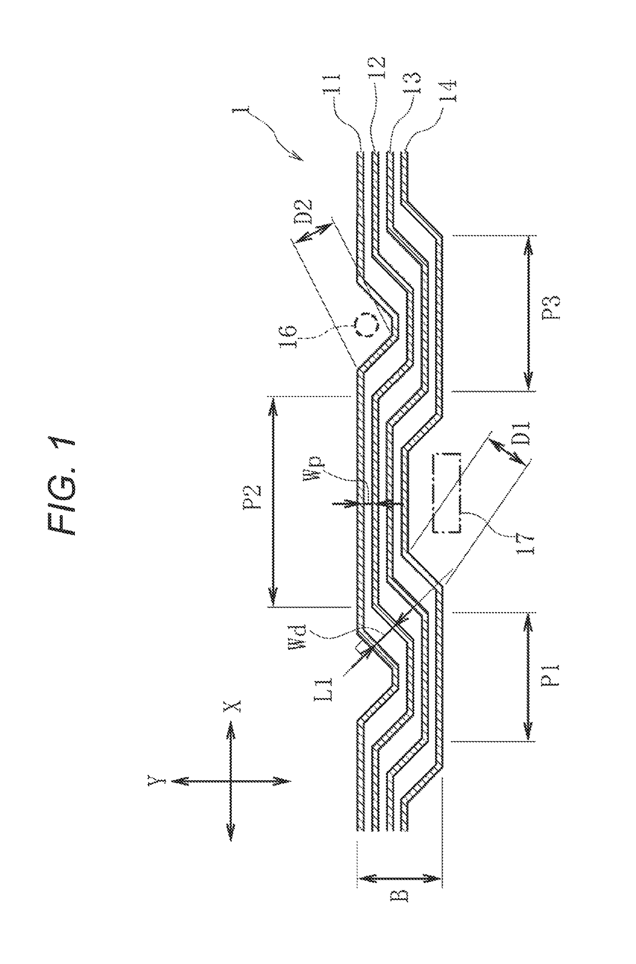
[0027]FIG. 1 illustrates a plan view of a wiring structure 1 of the disclosure. The wiring structure 1 is formed on the surface of a hard substrate or a flexible substrate to form a printed wiring substrate. In each drawing, an X direction represents a first direction, and a Y direction perpendicular to the X direction represents a second direction.
[0028]The wiring structure 1 includes a plurality of wiring patterns 11, 12, 13, and 14. The wiring patterns 11, 12, 13, and 14 are made of a conductive metal layer such as a copper foil.
[0029]The wiring structure 1 illustrated in FIG. 1 includes a first parallel wiring portion P1, a second parallel wiring portion P2, and a third parallel wiring portion P3. In the first parallel wiring portion P1, the second parallel wiring portion P2, and the third parallel wiring portion P3, at least two of the wiring patterns 11, 12, 13, and 14 are disposed to be linearly extended or paralleled to each other in the first direction (X direction). An int...
third embodiment
[0040]FIG. 4 illustrates a wiring structure 3 of the disclosure. In the wiring structure 3, the interval Wp between the wiring patterns 11, 12, and 13 in the parallel wiring portion is the same as those of the above embodiments. In a wiring path change portion D5, the respective wiring patterns 11, 12, and 13 are bent at a right angle.
[0041]Even in the wiring structure 3, the crosstalk noise can be reduced without increasing the width dimension in the Y direction.
[0042]FIG. 5 illustrates a part of a printed wiring substrate 20 on which the wiring structure 1 illustrated in FIG. 1 is applied.
[0043]The printed wiring substrate 20 includes a plurality of wiring patterns 21 in the surface of a hard or flexible substrate. In the wiring structure, there are provided the parallel wiring portions P10 and P11 and a wiring path change portion D11. In the wiring path change portion D11, the respective wiring patterns are extended at a slope intersecting with the first direction, and the wiring...
PUM
 Abstract
Description
Claims
Application Information
 - R&D
- Intellectual Property
- Life Sciences
- Materials
- Tech Scout
- Unparalleled Data Quality
- Higher Quality Content
- 60% Fewer Hallucinations
Browse by: Latest US Patents, China's latest patents, Technical Efficacy Thesaurus, Application Domain, Technology Topic, Popular Technical Reports.
© 2025 PatSnap. All rights reserved.Legal|Privacy policy|Modern Slavery Act Transparency Statement|Sitemap|About US| Contact US: help@patsnap.com


