In-cell touch display device and driving method thereof

a display device and in-cell technology, applied in the direction of instruments, computing, electric digital data processing, etc., can solve the problems of affecting the manufacturing yield rate, further degrading the touch sensitivity, and disassuring the measurement of capacitance change, so as to achieve enhanced integration of touch control and display functions, and simplify the structure

Active Publication Date: 2017-09-12
ILI TECHNOLOGY CORPORATION
View PDF3 Cites 2 Cited by
  • Summary
  • Abstract
  • Description
  • Claims
  • Application Information

AI Technical Summary

Benefits of technology

[0006]It is a primary object of the present invention to provide an in-cell touch display device and a driving method thereof. By performing touch sensing with intersected data lines and common lines, the in-cell touch display device and the driving method thereof of the present invention achieve a simplified structure as well as enhanced integration of touch control and display functions.
[0009]In the in-cell touch display device and the driving method thereof of the present invention, as the touch sensing elements are formed by intersected data lines and common lines in a common display panel, a simplified structure and a thinning effect are achieved. With a relatively smaller overlapping region between the common lines and the data lines, the background capacitance value is smaller and a ratio of the capacitance value contributed by a sensed object is greater. Therefore, with an appropriately designed background capacitance value, the touch sensing accuracy can be enhanced. Further, in the present invention, connection statuses of display control elements and touch control elements are switched through disposing switching elements, and a corresponding constant voltage is provided, thereby preventing interferences between display signals and touch signals.

Problems solved by technology

However, due to additional touch elements and corresponding production processes for the original display panel, the manufacturing yield rate is likely undesirably affected.
However, in the above solution, due to a larger overlapping region between the gate lines (and the connected gate electrodes) and the data lines (and the connected source electrodes) and a possible semiconductor layer disposed in between, an excessively large background capacitance is easily caused, hence disfavoring the measurement of the capacitance change and further degrading the touch sensitivity.

Method used


Image

  • In-cell touch display device and driving method thereof
  • In-cell touch display device and driving method thereof
  • In-cell touch display device and driving method thereof

Examples


Embodiment Construction

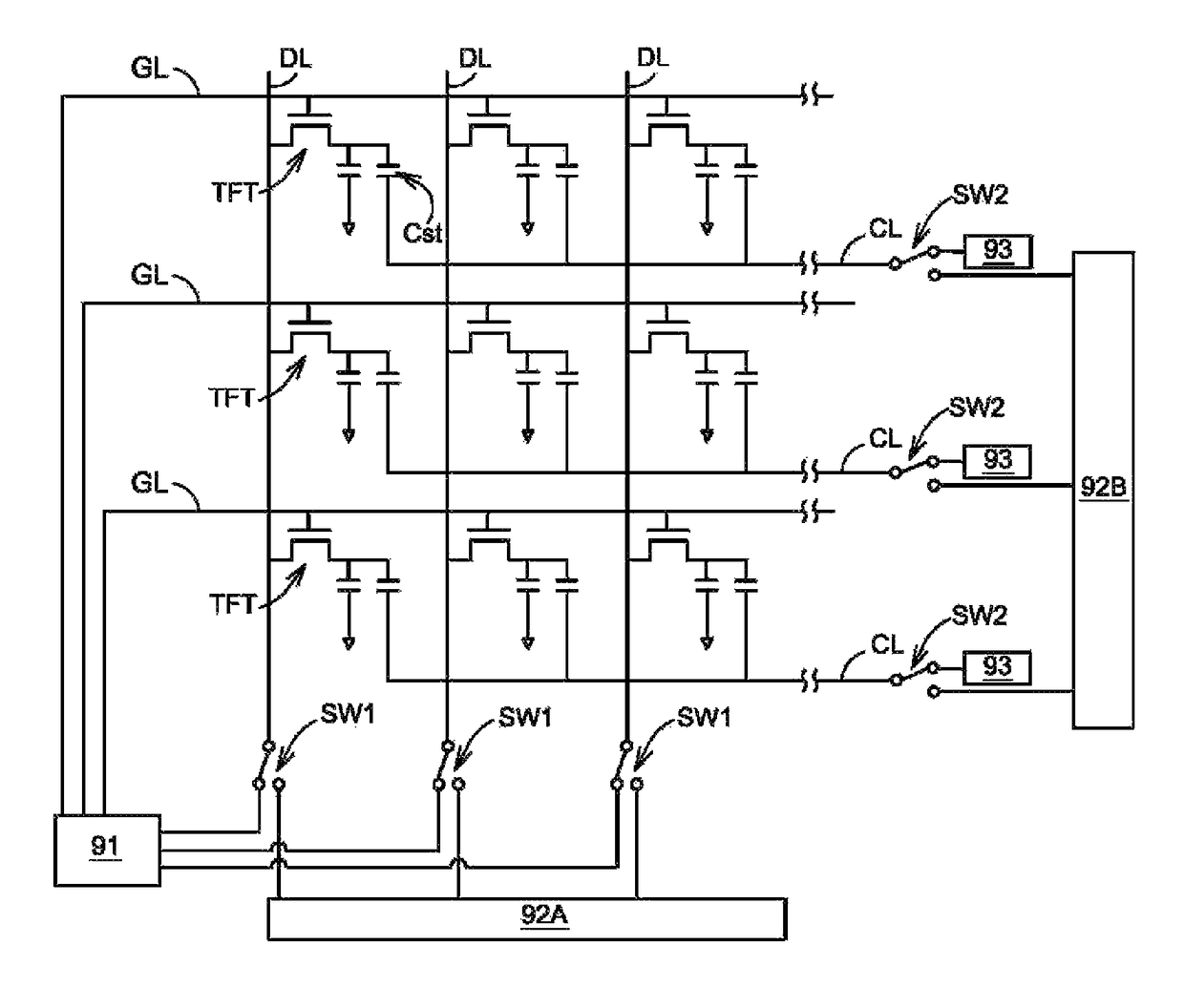
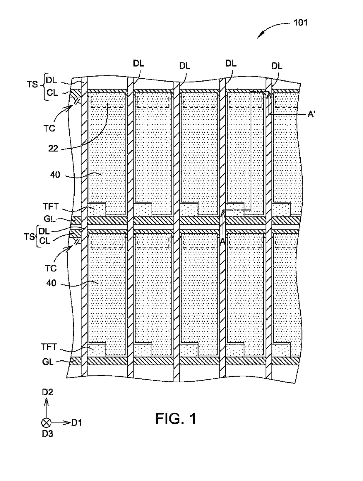
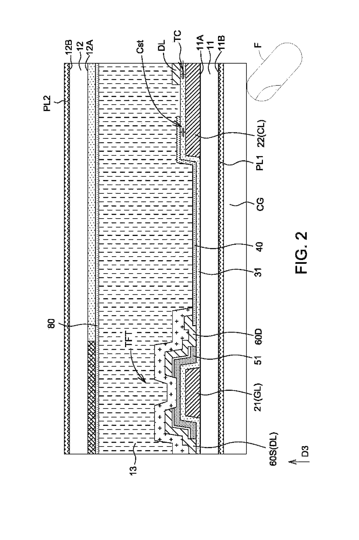
[0018]FIG. 1 to FIG. 4 show a schematic diagram, a section view and circuit diagrams of two different modes of an in-cell touch display device according to a first embodiment of the present invention, respectively. An in-cell touch display device 101 of the embodiment includes a first substrate 11, a second substrate 12, a liquid crystal layer 13, a plurality of data lines DL, a plurality of common lines CL, a plurality of gate lines GL, a plurality of first switching elements SW1, a plurality of second switching elements SW2, a first touch control element 92A, a second touch control element 92B, a display control element 91, and a common voltage source 93. The first substrate 11 has a first inner surface 11A and a first outer surface 11B. The second substrate 12 is disposed opposite the first substrate 11, and has a second inner surface 12A and a second outer surface 12B. The first inner surface 11A and the second inner surface 12A face each other. The liquid crystal layer 13 is di...


PUM


Abstract

An in-cell touch display device includes a first substrate, a plurality of common lines and a plurality of data lines. The common lines are disposed on the first substrate and extend along a first direction. The data lines are disposed on the first substrate and extend along a second direction. The common lines intersect and are insulated from the data lines. A plurality of touch sensing capacitors are formed at intersections of the common lines and the data lines to perform touch sensing.

Description

[0001]This application claims the benefit of U.S. Provisional Application Ser. No. 62 / 065,021, filed Oct. 17, 2014, the subject matter of which is incorporated herein by reference.BACKGROUND OF THE INVENTION[0002]Field of the Invention[0003]The invention relates in general to a touch display device and a driving method thereof, and more particularly to a touch display device that performs touch sensing using intersected data lines and common lines in a display panel, and a driving method thereof.[0004]Description of the Related Art[0005]Touch sensing technologies have been developed at a fast pace in the recently years. There are numerous consumer electronic products supporting a touch function commercially available. In such type of products, a region of an original display panel is assigned with a touch sensing function, i.e., an original simple display panel is converted to a touch display panel that supports a touch recognition function. According to different structural designs...

Claims


Application Information

Patent Timeline
Patent Type & Authority Patents(United States)
IPC IPC(8): G06F3/044G06F3/041
CPCG06F3/044G06F3/0412G06F3/0416G06F2203/04112G06F3/04184G06F3/0446G06F3/04166
Inventor HUNG, GUO-KIANGLIU, CHI KANG
Owner ILI TECHNOLOGY CORPORATION
Why Eureka
Try Eureka