Spectroscopic chemical analysis methods and apparatus

a spectroscopic and chemical analysis technology, applied in the direction of optical radiation measurement, fluorescence/phosphorescence, instruments, etc., can solve the problems of difficult to ensure stoichiometrical reactions, inconvenient operation, and large majority of chemicals that do not absorb strongly, so as to reduce weight

Active Publication Date: 2017-02-14
PHOTON SYST
View PDF1 Cites 20 Cited by
  • Summary
  • Abstract
  • Description
  • Claims
  • Application Information

AI Technical Summary

Problems solved by technology

A major drawback to the use of fluorescence detection is that the vast majority of chemicals do not absorb strongly at visible or infrared wavelengths where simple, inexpensive lasers emit.
This is highly inconvenient, especially at low analyte concentrations, and for compounds that lack appropriate functional groups.
For multifunctional compounds such as proteins, it is very difficult to ensure stoichiometrical reactions that can result in complex mixtures after derivatization.
Derivatization limits the types of molecules that can be studied, can lower overall detection sensitivity, reduces the ability to find unexpected analytes in complex mixtures, and may alter the very chemistry being studied.
These advantages were demonstrated using lasers that are unacceptable in a commercial instrument application because of their size, weight, power consumption, and / or cost.
It has been hampered as an analytical method by the fact that normal Raman scatter cross-sections of materials are typically very small.
Another problem that has hampered Raman spectroscopy as an analytical method is fluorescence background from many materials at wavelengths of interest in obtaining Raman spectra.
The problem remains that Raman scatter cross-sections in the infrared are small and powerful lasers are needed to obtain Raman spectral data.
In addition to their other problems, these powerful lasers sometimes cause sample damage.
But several major technical roadblocks have impeded progress in demonstrating sources which operate in the deep UV, especially at wavelengths less than about 300 nm.
The major roadblocks to producing deep UV semiconductor sources have been:1. the inability to adequately p-dope AlGaN materials with aluminum content greater than a few percent (i.e. measure as mole fraction);2. the inability to make low resistance, ohmic, contacts to AlGaN alloys with aluminum content greater than a few percent;3. Lattice mismatch with available substrate materials resulting in high defect density in active region;4. Inability to form facets with low losses at deep UV wavelengths; and5. Difficulty in forming waveguiding layers in high Al-content AlGaN alloys.

Method used


Image

  • Spectroscopic chemical analysis methods and apparatus
  • Spectroscopic chemical analysis methods and apparatus
  • Spectroscopic chemical analysis methods and apparatus

Examples


Embodiment Construction

Deep UV Radiation Production Methods and Sources

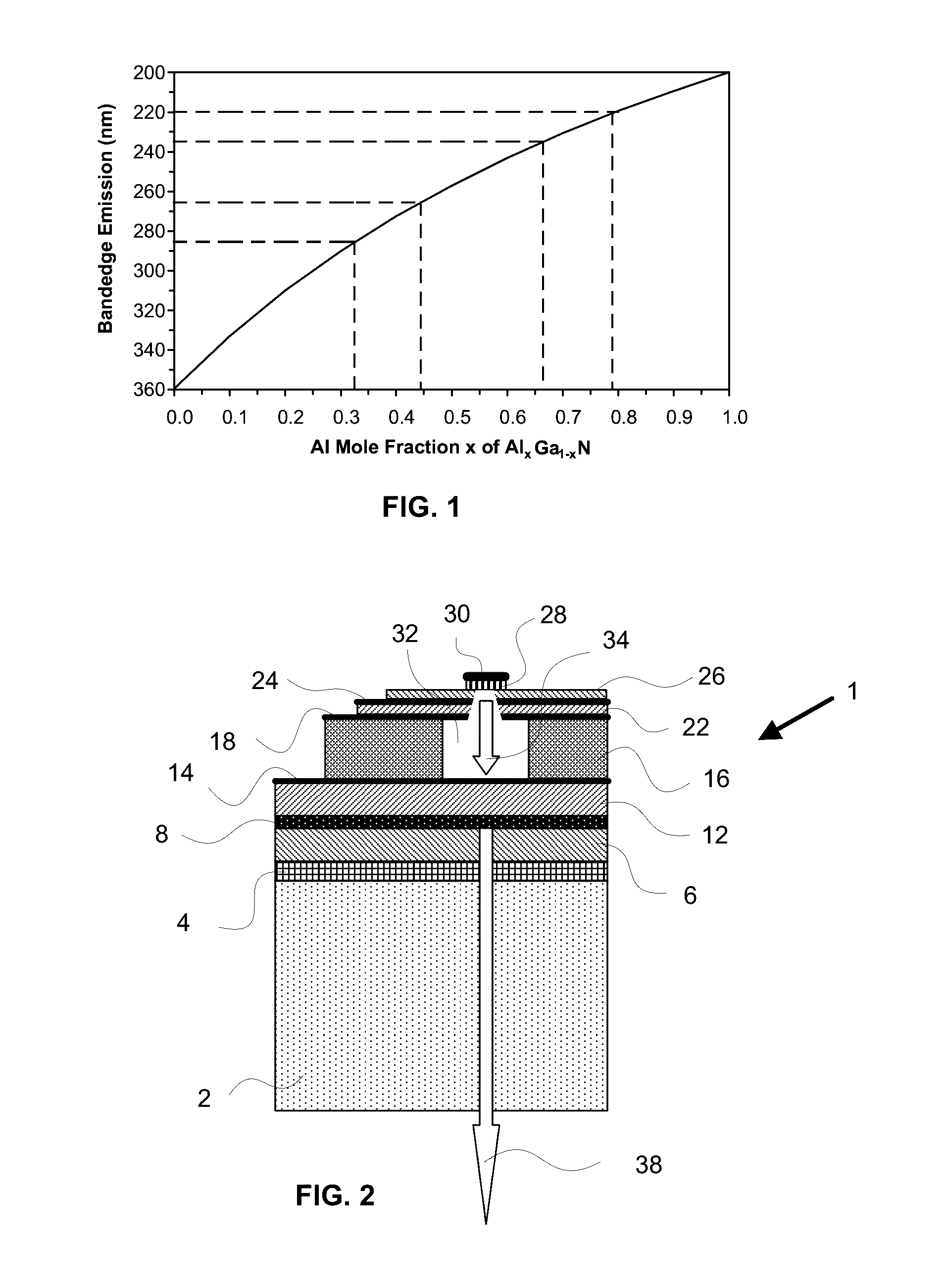
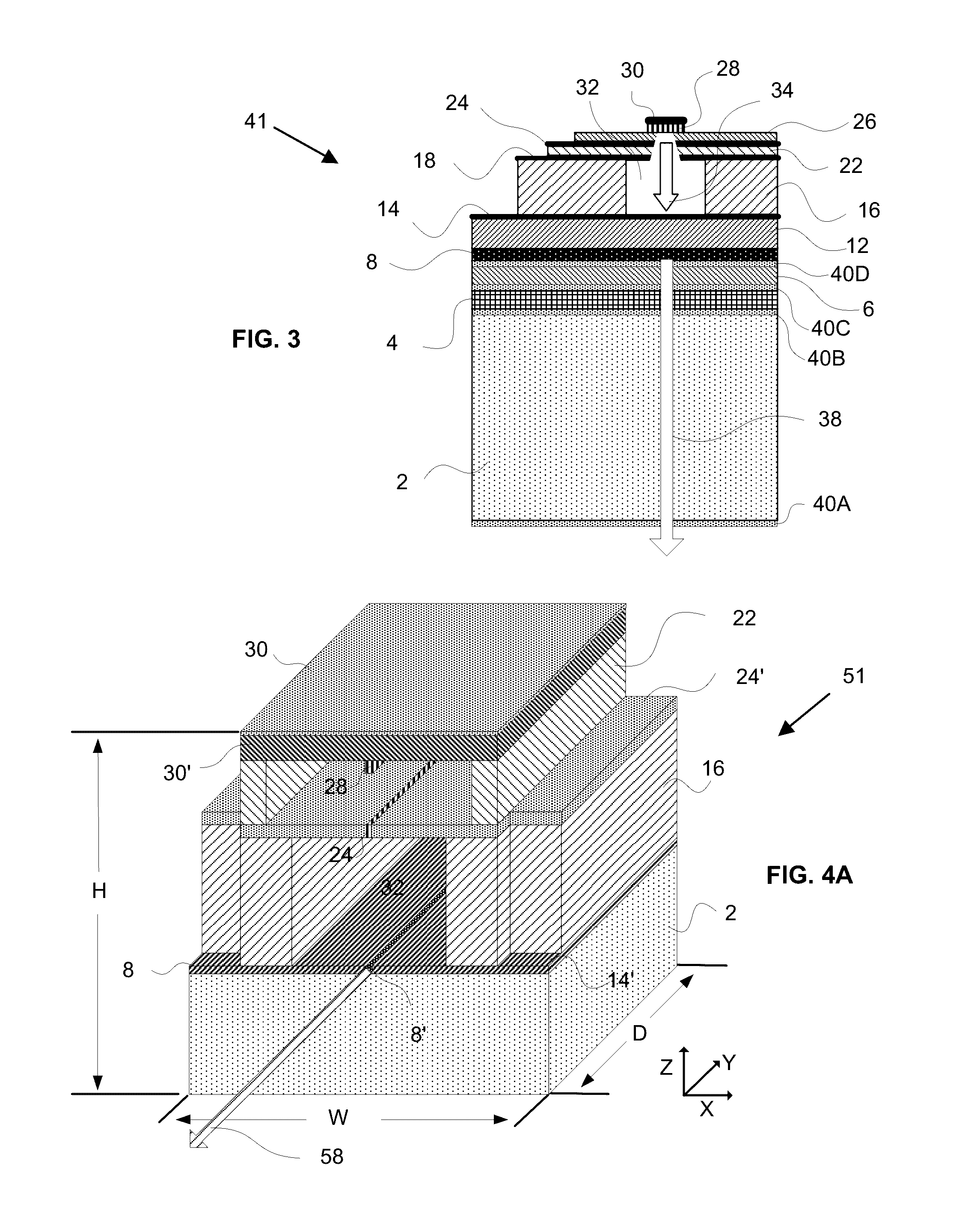
[0133]To avoid the difficulties, set forth above, related to producing deep UV semiconductor sources, Applicants have developed a pumping approach that uses ballistic electron beam injection directly into the active region of a wide band gap semiconductor material. One element that distinguishes some embodiments of the invention from the teachings about electron beam pumping noted above is that none of the publications discuss, describe, or suggest the use of wide bandgap semiconductor materials (i.e. semiconductor materials having a band gap greater than 3.5 eV, corresponding to wavelengths less than 400 nm, more preferably greater than 4.15 eV, corresponding to wavelengths less than 300 nm, and most preferably greater than 4.97 eV, corresponding to wavelengths less than 250 nm). Furthermore these references fail to teach the use of Group III nitride semiconductor material systems, such as an AlGaN alloy, for producing laser output us...


PUM

PropertyMeasurementUnit
wavelengthaaaaaaaaaa
weightaaaaaaaaaa

Abstract

Spectroscopic chemical analysis methods and apparatus are disclosed which employ deep ultraviolet (e.g. in the 200 nm to 300 nm spectral range) electron beam pumped wide bandgap semiconductor lasers, incoherent wide bandgap semiconductor light emitting devices, and hollow cathode metal ion lasers to perform non-contact, non-invasive detection of unknown chemical analytes. These deep ultraviolet sources enable dramatic size, weight and power consumption reductions of chemical analysis instruments. In some embodiments, Raman spectroscopic detection methods and apparatus use ultra-narrow-band angle tuning filters, acousto-optic tuning filters, and temperature tuned filters to enable ultra-miniature analyzers for chemical identification. In some embodiments Raman analysis is conducted along with photoluminescence spectroscopy (i.e. fluorescence and / or phosphorescence spectroscopy) to provide high levels of sensitivity and specificity in the same instrument.

Description

RELATED APPLICATIONS[0001]This application is a continuation of U.S. patent application Ser. No. 12 / 628,205 filed Nov. 30, 2009. The '205 application claims benefit of U.S. Patent Application No. 61 / 118,591, filed Nov. 28, 2008 and is a continuation-in-part of U.S. patent application Ser. No. 12 / 545,772, filed Aug. 21, 2009, which in turn is a continuation-in-part of U.S. patent application Ser. No. 12 / 399,743, filed Mar. 6, 2009 which in turn is a continuation of U.S. patent application Ser. No. 11 / 245,486 filed Oct. 5, 2005 which in turn claims benefit of U.S. Provisional Application No. 60 / 616,269, filed Oct. 5, 2004. Each of these applications is incorporated herein by reference as if set forth in full herein.US GOVERNMENT RIGHTS[0002]One or more of the inventions set forth herein were made with U.S. Government support under one or more of (1) NASA Contract No. NAS2-02086, (2) DARPA Contract No. W31 P4Q-04-C-R039, and / or (3) DTRA Contact No. HDTRA1-09-C-0010. The Government has ...

Claims


Application Information

Patent Timeline
Patent Type & Authority Patents(United States)
IPC IPC(8): G01N21/64G01J3/26G01N21/33G01N21/65
CPCG01N21/33G01N21/64G01N21/65G01N2201/06113G01N2201/068G01J3/10G01J3/36G01J3/44G01N27/44721G01N21/645G01N2021/6421G01N2021/6471G01N2201/0612G01N21/6486G01N2021/6419G01N2201/062
Inventor HUG, WILLIAM F.REID, RAY D.BHARTIA, ROHITLANE, ARTHUR L.
Owner PHOTON SYST
Why Eureka
Try Eureka