Gate driver for narrow bezel LCD
a technology of liquid crystal display and driver, which is applied in the field of flat panel display, can solve the problems of increasing the rc effect to consume much energy and fail, and achieve the effect of reducing the rc
- Summary
- Abstract
- Description
- Claims
- Application Information
AI Technical Summary
Benefits of technology
Problems solved by technology
Method used
Image
Examples
first embodiment
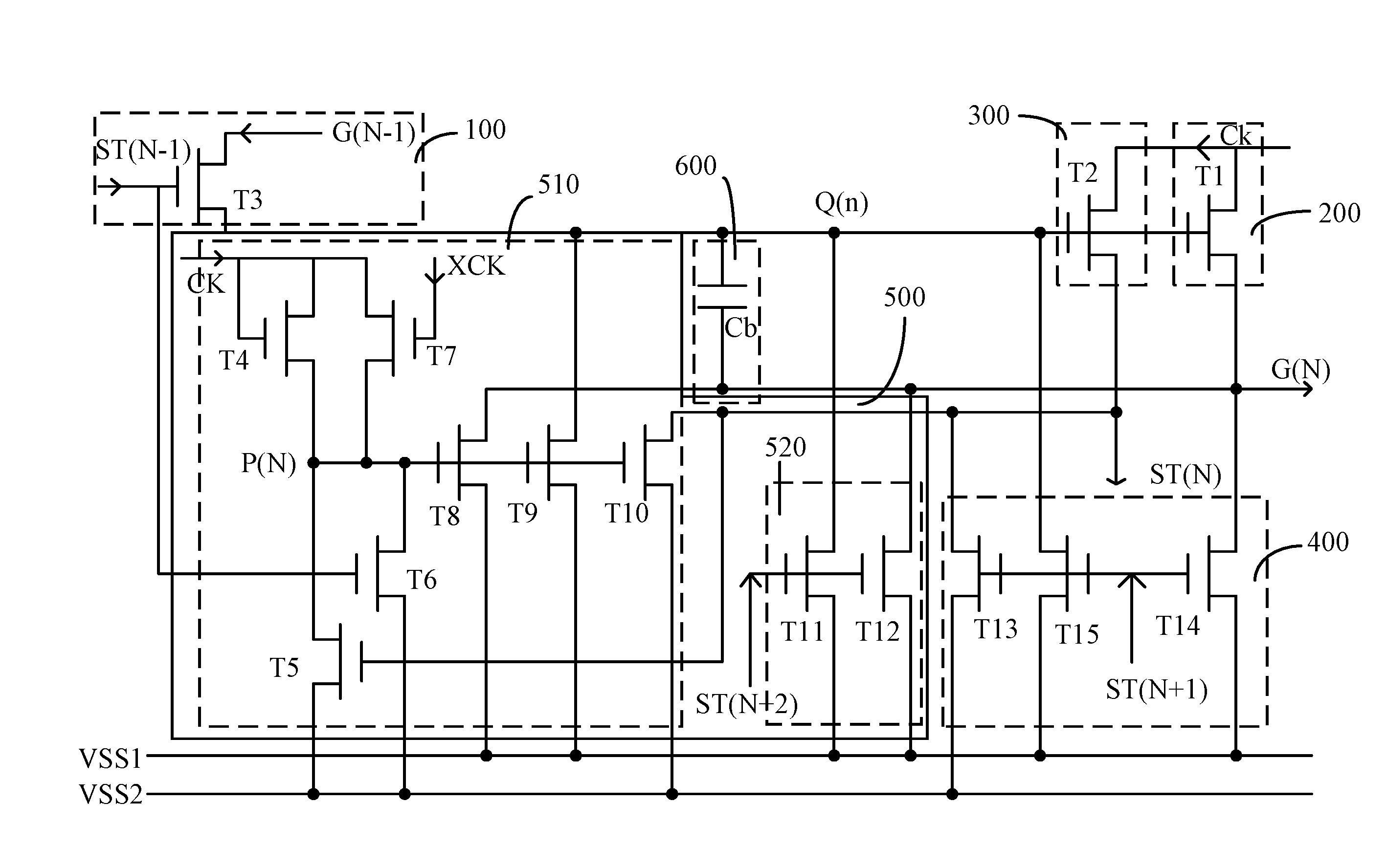
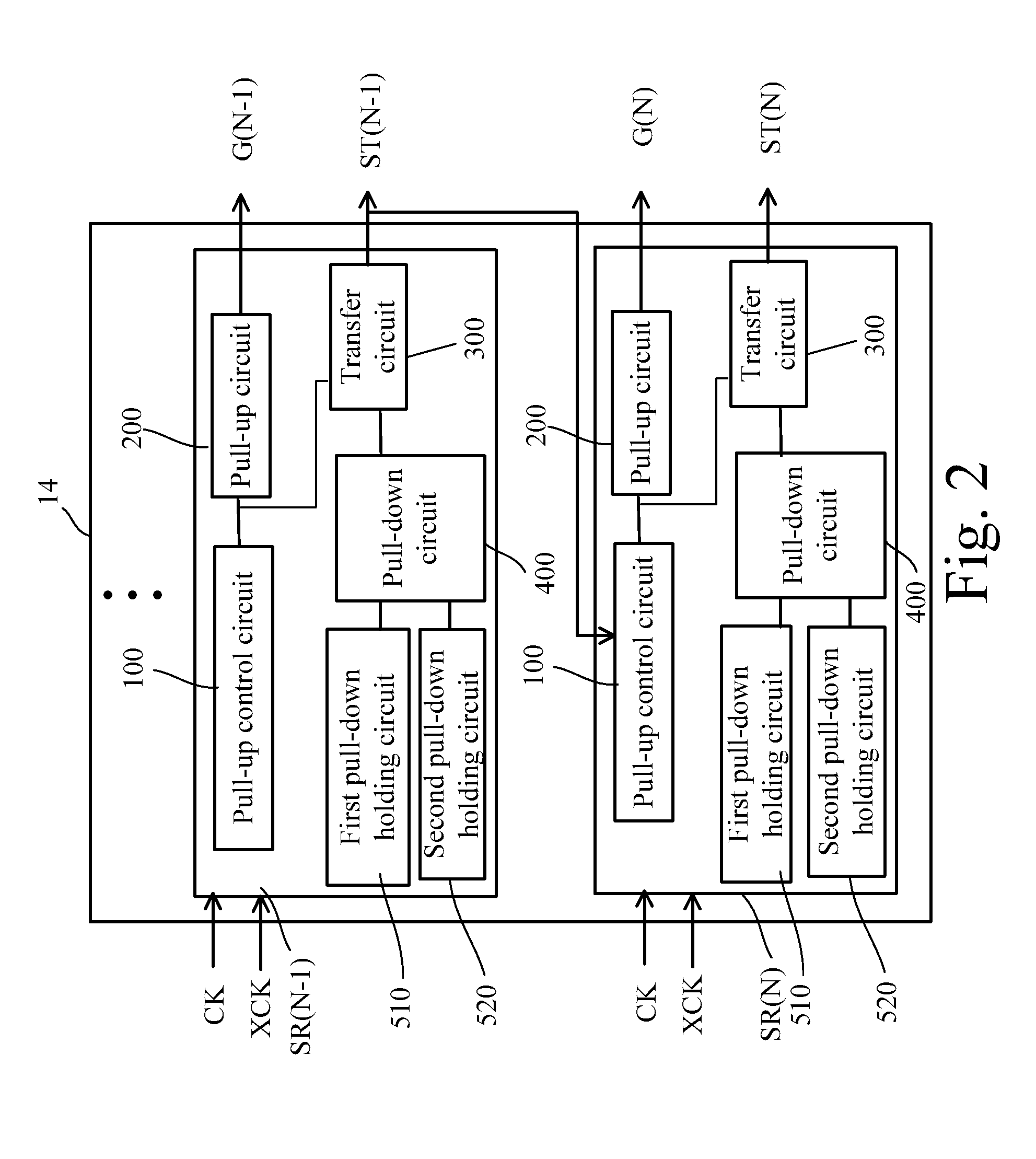
[0047]Refer to FIG. 3A, FIG. 3A is a circuit diagram of the shift register unit SR(N) shown in FIG. 2 according to the present invention. The pull-up circuit 200 may be a first transistor T1 whose a gate coupled to the first node Q(N), a source coupled to the first clock signal CK, a drain coupled to an output end G(N) for providing signal pulses to the output end G(N) based on the first clock signal CK. The transfer circuit 300 may be a second transistor T2 whose a gate coupled to the first node Q(N), a source coupled to the first clock signal CK, a drain coupled to a driving signal end ST(N) for providing driving signal pulses to the driving signal end ST(N) based on the first clock signal CK. The pull-up control circuit 100 is able to a third control circuit T3 whose a gate coupled to a driving signal end ST(N−1) of the previous one shift register unit SR(N−1), a drain coupled to the first node Q(N) for conducting the pull-up circuit 200 according to driving signal pulses of the ...
second embodiment
[0053]Please refer to FIG. 4A and FIG. 4B. FIG. 4A is a circuit diagram of the shift register unit shown in FIG. 2 according to the present invention. FIG. 4B is timing diagram of input signals, output signals, and voltages applied on nodes illustrated in FIG. 4A. The elements of the shift register unit SR(N) in FIG. 4A have the same labeled number with those of the shift register unit SR(N) in FIG. 3A have the identical operating principles, and no further description is demonstrated. A difference between the FIG. 4A and FIG. 3A is that the pull-down circuit 400 further comprises a sixteenth transistor T16, and the connections of the fifteenth transistor T15 and the sixteenth transistor T16 are not identical. A gate and a source of the fifteenth transistor T15 are respectively coupled to the driving signal end ST(n+1) of the next one shift register unit SR(n+1) for each shift register unit and to the first node Q(N). A gate and a source of the sixteenth transistor T16 are both coup...
third embodiment
[0054]Please refer to FIG. 5A and FIG. 5B. FIG. 5A is a circuit diagram of the shift register unit shown in FIG. 2 according to the present invention. FIG. 5B is timing diagram of input signals, output signals, and voltages applied on nodes illustrated in FIG. 5A. The elements of the shift register unit SR(N) in FIG. 5A have the same labeled number with those of the shift register unit SR(N) in FIG. 3A have the identical operating principles, and no further description is demonstrated. A difference between FIG. 5A and FIG. 3A is that the gate of the seventh transistor T7 of the first pull-down holding circuit 510 is coupled to the second node P(N) so that it reduces cross line crosstalk between the first clock signal CK and the second clock signal XCK. Compared with FIG. 3B, the second node P(N) discharges more effectively according to waveform of the seventh transistor T7. The operation principle and achieving effect of the shift register unit SR(N) in FIG. 5A is identical to which...
PUM
 Abstract
Description
Claims
Application Information
 - R&D
- Intellectual Property
- Life Sciences
- Materials
- Tech Scout
- Unparalleled Data Quality
- Higher Quality Content
- 60% Fewer Hallucinations
Browse by: Latest US Patents, China's latest patents, Technical Efficacy Thesaurus, Application Domain, Technology Topic, Popular Technical Reports.
© 2025 PatSnap. All rights reserved.Legal|Privacy policy|Modern Slavery Act Transparency Statement|Sitemap|About US| Contact US: help@patsnap.com


