
Process module for increasing the response of backside illuminated photosensitive imagers and associated methods

a technology of backside illumination and processing module, which is applied in the direction of wireless communication, radio frequency control device, assess restriction, etc., can solve the problems of silicon-based technologies for detecting infrared incident electromagnetic radiation, and achieve the effect of reducing specular reflection

Active Publication Date: 2016-11-15
SIONYX
View PDF538 Cites 6 Cited by
  • Summary
  • Abstract
  • Description
  • Claims
  • Application Information

AI Technical Summary

Benefits of technology

This patent describes a surface featuring technology with specific criteria for its size and spacing. The features have a specific center-to-center distance of one half wavelength of light or multiples of this distance, depending on the refractive index of the surrounding material. The features have a uniform spacing across a textured region and also a specific height of about a multiple of a quarter wavelength of light. The surface features can be designed to reduce specular reflection. Overall, this technology allows for precise and uniform control over the size and spacing of surface features, which can be useful in various applications such as optical devices and communication systems.

Problems solved by technology

Silicon-based technologies for detecting infrared incident electromagnetic radiation have been problematic, however, because silicon is an indirect bandgap semiconductor having a bandgap of about 1.1 eV.

Method used


Image

  • Process module for increasing the response of backside illuminated photosensitive imagers and associated methods
  • Process module for increasing the response of backside illuminated photosensitive imagers and associated methods
  • Process module for increasing the response of backside illuminated photosensitive imagers and associated methods

Examples


Embodiment Construction

[0030]Before the present disclosure is described herein, it is to be understood that this disclosure is not limited to the particular structures, process steps, or materials disclosed herein, but is extended to equivalents thereof as would be recognized by those ordinarily skilled in the relevant arts. It should also be understood that terminology employed herein is used for the purpose of describing particular embodiments only and is not intended to be limiting.

[0031]Definitions

[0032]The following terminology will be used in accordance with the definitions set forth below.

[0033]It should be noted that, as used in this specification and the appended claims, the singular forms “a,” and, “the” include plural referents unless the context clearly dictates otherwise. Thus, for example, reference to “a dopant” includes one or more of such dopants and reference to “the layer” includes reference to one or more of such layers.

[0034]As used herein, “tuning” refers to selectively enhancing a d...


PUM


Abstract

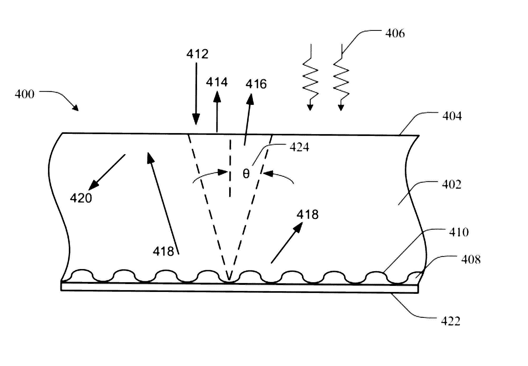
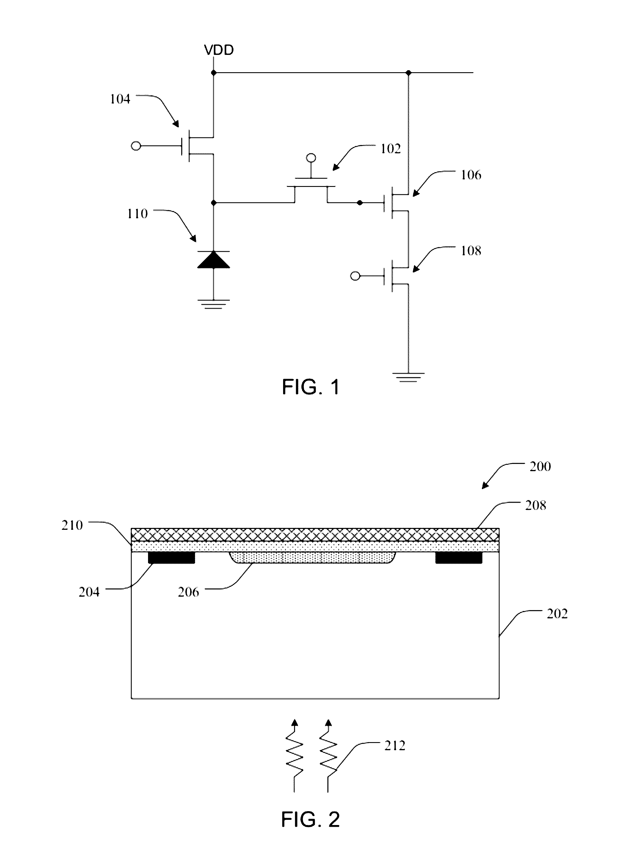
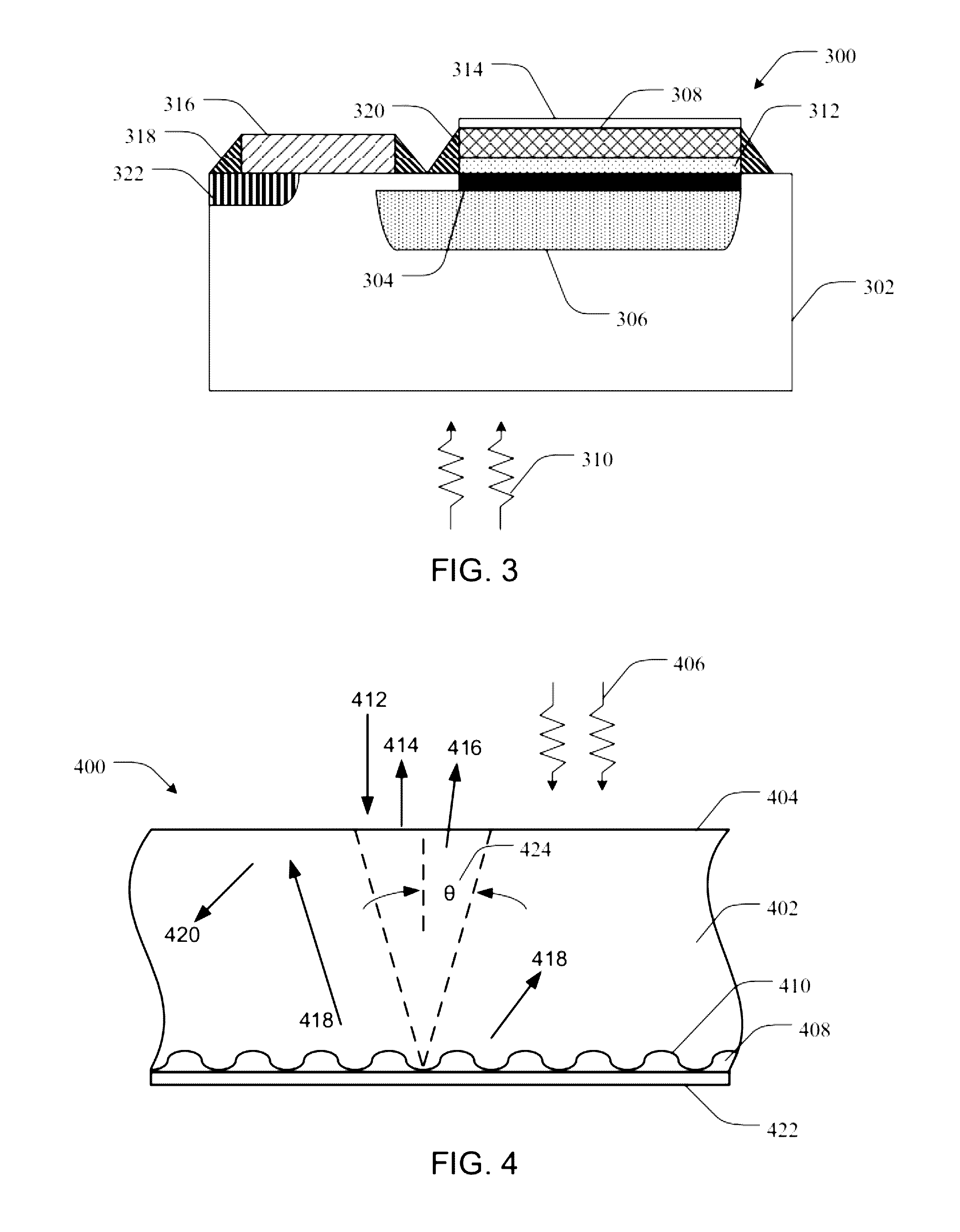
Backside illuminated photosensitive devices and associated methods are provided. In one aspect, for example, a backside-illuminated photosensitive imager device can include a semiconductor substrate having multiple doped regions forming a least one junction, a textured region coupled to the semiconductor substrate and positioned to interact with electromagnetic radiation where the textured region includes surface features sized and positioned to facilitate tuning to a preselected wavelength of light, and a dielectric region positioned between the textured region and the at least one junction. The dielectric region is positioned to isolate the at least one junction from the textured region, and the semiconductor substrate and the textured region are positioned such that incoming electromagnetic radiation passes through the semiconductor substrate before contacting the textured region. Additionally, the device includes an electrical transfer element coupled to the semiconductor substrate to transfer an electrical signal from the at least one junction.

Description

PRIORITY DATA[0001]This application claims the benefit of U.S. Provisional Application Ser. No. 61 / 495,243, filed on Jun. 9, 2011, which is incorporated herein by reference.BACKGROUND[0002]The interaction of light with semiconductor materials has been a significant innovation. Silicon imaging devices are used in various technologies, such as digital cameras, optical mice, video cameras, cell phones, and the like. Charge-coupled devices (CCDs) were widely used in digital imaging, and were later improved upon by complementary metal-oxide-semiconductor (CMOS) imagers having improved performance. Many traditional CMOS imagers utilize front side illumination (FSI). In such cases, electromagnetic radiation is incident upon the semiconductor surface containing the CMOS devices and circuits. Backside illumination CMOS imagers have also been used, and in many designs electromagnetic radiation is incident on the semiconductor surface opposite the CMOS devices and circuits. CMOS sensors are ty...

Claims


Application Information

Patent Timeline
Patent Type & Authority Patents(United States)
IPC IPC(8): H01L27/00H01L27/146H01L31/0232H01L31/18
CPCH01L27/1464H01L27/1462H01L27/14629H01L31/0232H01L31/18H01L27/14685H01L27/14689H01L27/14692H04H20/57H04H20/59H04H20/72H04W4/90H04W48/16
Inventor HADDAD, HOMAYOONMCKEE, JEFFREYJIANG, JUTAOMILLER, DRAKEPALSULE, CHINTAMANIFORBES, LEONARD
Owner SIONYX
Learn More