Method of manufacturing a solar cell and equipment therefore

a manufacturing method and technology of solar cells, applied in photovoltaic energy generation, electrical equipment, renewable energy products, etc., can solve the problems of increasing the cost of solar cells produced, adding significant cost to machine sales price, and increasing the complexity of machines, so as to reduce the efficiency loss due to charge carrier recombination, reduce the concentration of doping, and improve the effect of efficiency

Inactive Publication Date: 2016-11-08
TEMPRESS IP
View PDF10 Cites 0 Cited by
  • Summary
  • Abstract
  • Description
  • Claims
  • Application Information

AI Technical Summary

Benefits of technology

[0011]It is another object to provide an improved semiconductor equipment and use thereof, with reduced machine complexity. It is a further object of the invention to provide a solar cell with an interdigitated back contact (IBC) with appropriate resolution.
[0040]This solar cell is the result of overetching and has the advantage of creating a second subregion with a relatively large area suitable as contact region in comparison to the underlying substrate support. The lateral protrusion of the first subregion over the substrate ‘neck’ is suitable in view of the subsequent deposition of contacts, typically by means of low(er) resolution processes such as screen printing or electroplating that are suitable for assembly processes, and wherein resistive losses are to be as small as possible. Nevertheless, the structure still has a relatively small interface between the contact region and the rest of the substrate. This is suitable to reduce recombination losses that are known to reduce efficiency of the solar cell operation. A further advantage is that the lateral protrusion allows anchoring of subsequent layers and therewith better adhesion, particularly with layers of polymer materials.

Problems solved by technology

The technique has a disadvantage in that the installation and maneuvering of shadow masks inside the implanter adds to the complexity of the machine and therefore adds significant cost to the machine sales price.
Through depreciation the additional machine complexity then adds to the cost of the produced solar cells.
Another disadvantage is that these shadow masks heat up quite a bit during continuous use in an ion implanter and will therefore generally change shape to some extent.
Another disadvantage of shadow masking is that the masks themselves cannot make any arbitrary shape because the mask needs to be able support itself.
For this reason, the patterns made on the semiconductor substrates are limited in their design.

Method used


Image

  • Method of manufacturing a solar cell and equipment therefore
  • Method of manufacturing a solar cell and equipment therefore
  • Method of manufacturing a solar cell and equipment therefore

Examples


Embodiment Construction

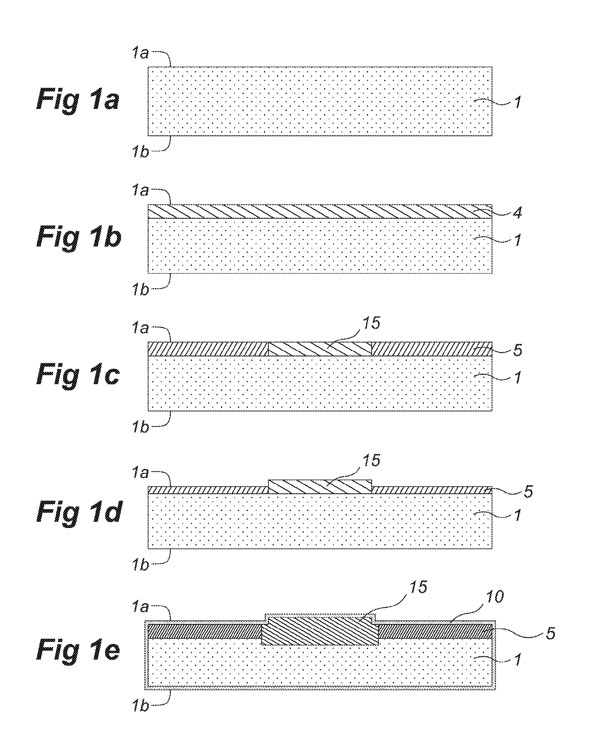
[0051]The Figures are diagrammatical in nature and not drawn to scale. The Figures are purely intended for illustrative purpose. Equal reference numerals in different Figures refer to same or similar elements.

[0052]FIG. 1a-c shows in a cross-sectional view a first embodiment of the method, resulting in a partial removal of the first subregion to a predefined depth.

[0053]FIG. 1a shows a semiconductor substrate 1 with a first side 1a and a second side 1b. The semiconductor substrate 1 is preferably a silicon substrate, such as a multicrystalline substrate or most preferably a monocrystalline silicon substrate that is doped with either n-type or p-type charge carriers as known per se to the skilled person. The semiconductor substrate suitably has a thickness of up to 200 micrometers. In the event that the semiconductor substrate is intended for the manufacture of a solar cell, the side 1a, 1b of the substrate 1 being intended for use as the front side is typically texturized in known m...


PUM


Abstract

Methods of manufacturing a solar cell are provided. Aspects of embodiments of the methods include introducing charge carriers into a substrate on a first side by ion implantation to produce an amorphized region followed by selectively recrystallizing material in part of the amorphized region to define a first recrystallized subregion and then at least partially removing recrystallized material from the first subregion. An apparatus for carrying out said method and a resulting solar cell having surface topology are also provided.

Description

FIELD OF THE INVENTION[0001]The invention relates to a method of manufacturing a solar cell, said device comprising a semiconductor substrate with a first side and an opposed second side, at which first side an active region doped with charge carriers of a first conductivity type is defined selectively, comprising creating first and second subregions at the first side with a mutually different amount of charge carriers, whereto said charge carriers are introduced into the substrate on said first side by ion implantation,[0002]The invention also relates to a semiconductor equipment for the selective creation of an active region comprising charge carriers of a first conductivity type at a first side of a semiconductor substrate, said equipment comprising a ion implanter suitable for implantation at a dose level that induces surface amorphization of the semiconductor substrate to define an amorphized region.[0003]The invention further relates to a solar cell comprising a semiconductor ...

Claims


Application Information

Patent Timeline
Patent Type & Authority Patents(United States)
IPC IPC(8): H01L31/18H01L31/065H01L31/068H01L31/20
CPCH01L31/1872H01L31/065H01L31/0682H01L31/1804H01L31/1864H01L31/20Y02E10/547Y02P70/521Y02P70/50
Inventor NABER, RONALD CORNELIS GERARD
Owner TEMPRESS IP
Why Eureka
Try Eureka