Organic light emitting diode display

a light-emitting diode and organic technology, applied in the direction of electrical equipment, semiconductor devices, instruments, etc., can solve the problems of difficult control of the gate voltage vgs of driving thin-film transistors, and achieve the effects of improving display quality, ensuring storage capacitance, and increasing resolution of organic light-emitting diodes

Active Publication Date: 2016-09-20
SAMSUNG DISPLAY CO LTD
View PDF25 Cites 32 Cited by
  • Summary
  • Abstract
  • Description
  • Claims
  • Application Information

AI Technical Summary

Benefits of technology

The described technology improves the display quality of organic light emitting diode displays by broadening the driving range of a driving thin film transistor, which leads to more precise control of the gray level of light emitted from the OLED. Other improvements include ensuring sufficient storage capacitance even at a high resolution, avoiding or preventing low gray level stains, and improving the overall display performance.

Problems solved by technology

Therefore, it may be difficult to control the magnitude of the gate voltage Vgs of the driving thin film transistor to ensure a large number of gray levels.

Method used


Image

  • Organic light emitting diode display
  • Organic light emitting diode display
  • Organic light emitting diode display

Examples


Embodiment Construction

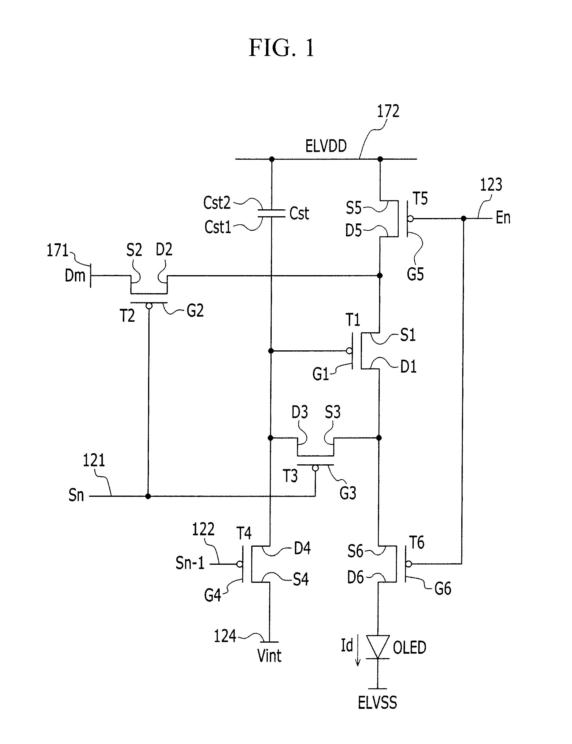
[0055]Hereinafter, embodiments of the present invention will be described more fully with reference to the accompanying drawings, in which exemplary embodiments of the invention are shown. As those skilled in the art would realize, the described embodiments may be modified in various ways, all without departing from the spirit or scope of the present invention.

[0056]To describe embodiments of the present invention, portions that do not relate to the description are omitted, and same or like constituent elements are designated by same reference numerals throughout the specification.

[0057]In addition, the size and thickness of each component shown in the drawings may be arbitrarily shown for understanding and ease of description, but the present invention is not limited thereto. In the drawings, the thickness of layers, films, panels, regions, areas, etc., may be exaggerated for clarity, for understanding, and for ease of description. It will be understood that when an element such as...


PUM


Abstract

An organic light emitting diode display includes a substrate, a scan line on the substrate for transferring a scan signal, a data line crossing the scan line and for transferring a data signal, a driving voltage line crossing the scan line and for transferring a driving voltage, a switching thin film transistor coupled to the scan line and the data line, a driving thin film transistor coupled to a switching drain electrode of the switching thin film transistor, and an organic light emitting diode (OLED) coupled to a driving drain electrode of the driving thin film transistor, wherein a driving semiconductor layer of the driving thin film transistor is bent and in a plane substantially parallel to the substrate.

Description

CROSS-REFERENCE TO RELATED APPLICATION[0001]This application claims priority to and the benefit of Korean Patent Application No. 10-2012-0084976 filed in the Korean Intellectual Property Office on Aug. 2, 2012, the entire content of which are incorporated herein by reference.BACKGROUND[0002]1. Field[0003]The described technology relates generally to an organic light emitting diode display.[0004]2. Description of Related Art[0005]An organic light emitting diode display includes two electrodes and an organic emission layer interposed therebetween, electrons injected from one electrode and holes injected from the other electrode are combined with each other in the organic emission layer to form an exciton, and light is emitted while the exciton discharges energy.[0006]The organic light emitting diode display includes a plurality of pixels, each including an organic light emitting diode that is a self-light emitting element, and a plurality of thin film transistors and capacitors for dr...

Claims


Application Information

Patent Timeline
Patent Type & Authority Patents(United States)
IPC IPC(8): H01L27/32G09G3/32
CPCH01L27/3297H01L27/3262H01L27/3276G09G3/3225H01L27/3265H01L27/124H01L27/1255H10K59/123H10K59/1216H10K59/124H10K59/1213H10K59/131G09G3/3655G09G2300/0847G09G2300/0809
Inventor KIM, SE-HOPARK, JIN-WOOLEE, WON-SE
Owner SAMSUNG DISPLAY CO LTD
Why Eureka
Try Eureka