Method for capacitively reading resistive memory elements and nonvolatile, capacitively readable memory elements for implementing the method

a capacitively readable, memory element technology, applied in information storage, static storage, digital storage, etc., can solve the problem of limiting the maximum array size that can be implemented, the symmetry of the switching behavior of such memory elements is worsened, and the type of manufacture is technologically very complex, etc. problem, to achieve the effect of low leakage current, low leakage current and high leakage curren

Active Publication Date: 2016-09-13
FORSCHUNGSZENTRUM JULICH GMBH +1
View PDF13 Cites 0 Cited by
  • Summary
  • Abstract
  • Description
  • Claims
  • Application Information

AI Technical Summary

Benefits of technology

[0012]It was furthermore found that the second memory cell becomes indispensable for the memory function when the capacitive read-out method is used. The second memory cell was originally introduced into the memory elements according to German patent 10 2009 023 153 so as to provide a high-resistance resistor for parasitic current paths through non-addressed memory elements in a matrix, during read-out using a read current through the memory element. If reading out is carried out capacitively without read current, this is no longer a factor. By now implementing a fixed capacitance in a considerably simpler and more compact design than a second memory cell, the same information can be stored in a smaller space at lower costs, without the problem of parasitic current paths returning.
[0019]According to the invention, the fixed capacitance comprises the gate dielectric of a field effect transistor. This field effect transistor can in particular be a MOSFET or the storage transistor of a flash or EEPROM memory. For example, the resistive memory cell, instead of a metallic gate, can be applied to the gate dielectric covering the semiconducting channel of the transistor. The memory element has the advantage that the field effect transistor acts as both the activating electronic device and as a very sensitive read-out electronic device for the memory cell.
[0025]In contrast to storage transistors of EEPROM or flash memories, however, the gate dielectric need not be designed to ensure that the charge stored on the floating gate is maintained for a long time. The gate dielectric thus does not have to ensure the non-volatility which, according to the invention, is already inherent in the resistive memory cell. As a result, the gate dielectric can have a thinner design, so that electrons can tunnel through the dielectric already at lower write voltages and drive a current pulse through the memory cell, which switches the cell.
[0026]For the resistive memory cell to be switchable, the gate dielectric must be subject to leakage current. The consequence of this is that the leakage current IG between the gate and source is dependent on the stored state of the resistive memory cell. If this cell is in the state LRS, the leakage current is high; if it is in the state HRS, the leakage current is low. This conflicts with the customary goal that is pursued in the development of transistors of minimizing the leakage current IG, which increases both power consumption and heat development.
[0030]An antiserial series connection moreover offers added degrees of freedom for a circuitry-related optimization, for example to increase the switching voltage. For this purpose, in particular the inherent center electrode between the two memory cells A and B can be used. For example, a series resistor can be installed in the series connection. An increase in the switching voltage can be useful, for example, in valence change resistive memories based on CMOS-compatible materials, such as Ta2O5 or HfO2, so that the resistive memory does not undesirably change state as a result of a read access.

Problems solved by technology

This is a limiting factor for the maximum array size that can be implemented.
The drawback is that this type of manufacture is technologically very complex and worsens the symmetry of the switching behavior of such memory elements.

Method used


Image

  • Method for capacitively reading resistive memory elements and nonvolatile, capacitively readable memory elements for implementing the method
  • Method for capacitively reading resistive memory elements and nonvolatile, capacitively readable memory elements for implementing the method
  • Method for capacitively reading resistive memory elements and nonvolatile, capacitively readable memory elements for implementing the method

Examples


Embodiment Construction

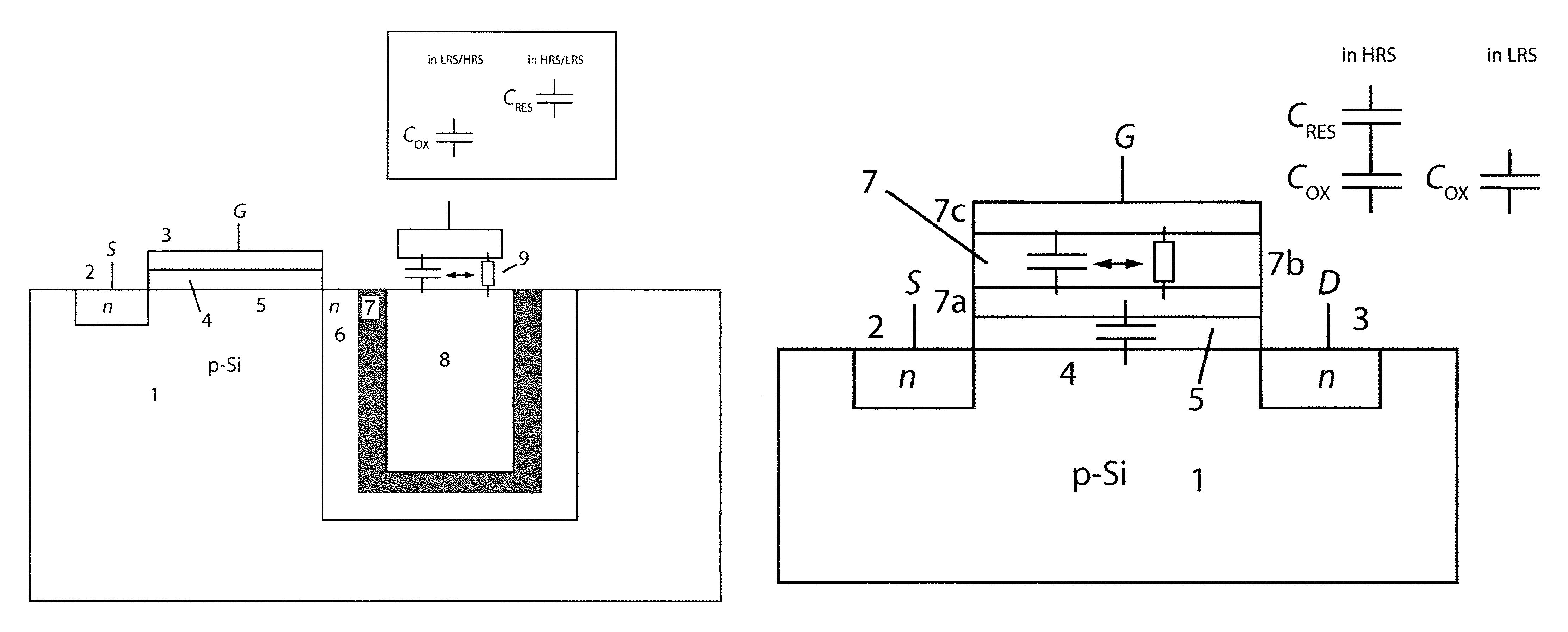
[0045]FIG. 1 schematically shows the composition of a memory element according to the invention, which was implemented as a series connection of a DRAM memory cell with a resistive memory cell. The transistor of the DRAM cell comprising an n-doped source region 2, a gate 3 that is insulated by a gate dielectric 4 from the p-doped channel 5, and an n-doped drain region 6 is introduced into a substrate 1 made of p-doped silicon. So as to produce the drain region 6, initially a trench was introduced into the substrate 1, and the wall of this trench was subsequently n-doped. When a voltage is applied between the source 2 and the gate 3, the channel 5 becomes n-conducting, which activates the transistor.

[0046]SiO2, which may also be replaced by another dielectric, was applied as the dielectric 7 to the trench wall forming the drain region 6. The trench was then filled with n-doped silicon 8, which may also be replaced by a metal. This silicon 8 and the drain region 6 constitute the plate...


PUM


Abstract

A method for reading out a non-volatile memory element having at least two stable states 0 and 1. This memory element comprises at least one resistive memory cell, which encodes the two states 0 and 1 into a state HRS having higher electrical resistance and a state LRS having lower electrical resistance. In the two states 0 and 1, the memory element has differing capacitances C0,1; this difference is used to determine which state is present. A memory element is selected in which a fixed capacitance that is independent of the state of the memory cell is connected in series with the memory cell. A series connection of a resistive memory cell with a fixed capacitance, instead of with a second resistive memory cell, improves the signal strength during capacitive read-out. The second memory cell becomes indispensable for the memory function when the memory element is read out capacitively. Moreover memory elements were developed which combine a field effect transistor or a DRAM structure with a resistive memory cell or an antiserial series connection of such memory cells.

Description

[0001]The invention relates to a method for capacitively reading out resistive memory elements and to non-volatile, capacitively readable memory elements for carrying out the method.BACKGROUND OF THE INVENTION[0002]Compared to charge-based memories, such as flash memories, passive resistive memory cells have a simpler design and can therefore be implemented on an ideal surface area of 4F2 at a given minimal feature size F. However, in a large array comprising many such memory cells, not only do currents flow through the above-mentioned memory cell, but there are also parasitic current paths through memory cells that have not been mentioned. This is a limiting factor for the maximum array size that can be implemented.[0003]It is known from German patent 10 2009 023 153 to design a resistively switching memory element as an antiserial circuit that is composed of two memory cells. Each such memory element forms a high-resistance resistor, regardless of the state of the element (0 or 1)...

Claims


Application Information

Patent Timeline
Patent Type & Authority Patents(United States)
IPC IPC(8): G11C14/00G11C13/00G11C11/56G11C11/16
CPCG11C14/0045G11C11/5685G11C13/003G11C13/004G11C11/16G11C2213/53G11C2213/74G11C2213/76G11C2213/79
Inventor TAPPERTZHOFEN, STEFANLINN, EIKENIELEN, LUTZWASER, RAINERVALOV, ILIA
Owner FORSCHUNGSZENTRUM JULICH GMBH
Why Eureka
Try Eureka