Eureka AIR delivers breakthrough ideas for toughest innovation challenges, trusted by R&D personnel around the world.

Layer transfer of films utilizing controlled shear region

a film and shear region technology, applied in the field of film layer transfer, can solve the problems of poor carrier life, many limitations of solar cells, and difficult manufacturing of materials for solar cells, and achieve the effects of high efficiency, reduced kerf loss, and high quality

Active Publication Date: 2016-06-07
SILICON GENERAL CORPORATION
View PDF350 Cites 10 Cited by
  • Summary
  • Abstract
  • Description
  • Claims
  • Application Information

AI Technical Summary

Benefits of technology

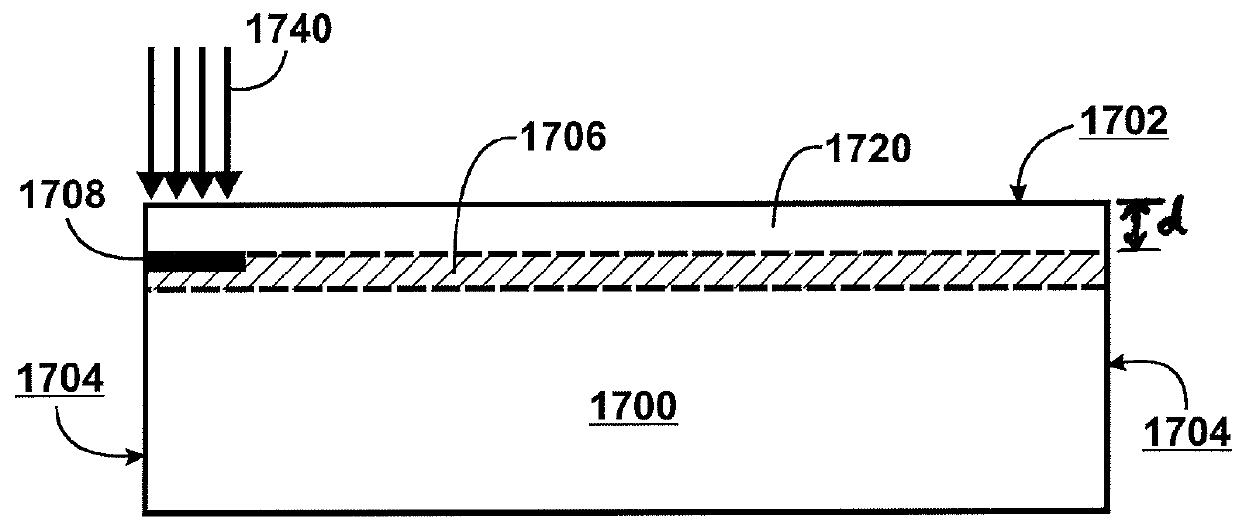
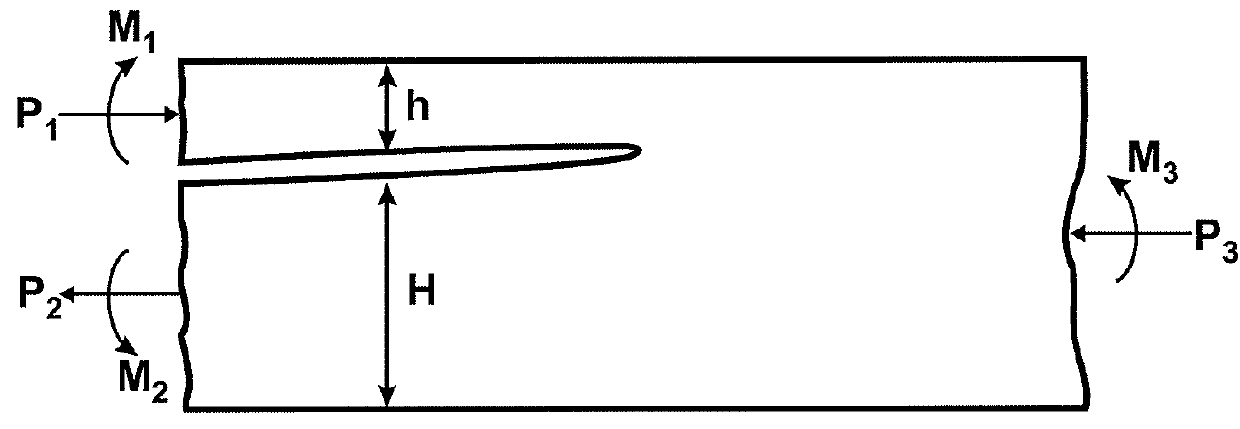
[0010]A film of material may be formed by providing a semiconductor substrate having a surface region and a cleave region located at a predetermined depth beneath the surface region. During a process of cleaving the film from the substrate, shear in the cleave region is carefully controlled. According to certain embodiments, an in-plane shear component (KII) is maintained near zero, sandwiched between a tensile region and a compressive region. In one embodiment, cleaving can be accomplished using a plate positioned over the substrate surface. The plate serves to constrain movement of the film during cleaving, and together with a localized thermal treatment reduces shear developed during the cleaving process. According to other embodiments, the KII component is purposefully maintained at a high level and serves to guide and drive fracture propagation through the cleave sequence. In one embodiment, the high KII component is achieved by adiabatic heating of silicon through exposure to E-beam radiation, which imparts a highly abrupt thermal gradient and resulting stress at a precisely defined depth in the silicon.
[0012]Many benefits can be obtained by implementing the present invention. In a preferred embodiment, single crystal silicon ingot substrate with a surface plane in an {111} or {110} crystallographic plane can be selected. Thus, the ion implantation process for creating cleave region can be mostly eliminated or limited to form a cleave initiation region with a portion of peripheral region. This substantially simplifies the layer transfer process, reduces system energy cost and increases productivity.
[0013]In certain embodiments, the process is divided into (i) an initiation process utilizing a higher implant dose (the initiation dose) to initiate a fracture in a relatively small area of the silicon ingot substrate (the initiation region), and (ii) a propagation process that extends the initiated crack tip through the remainder of the silicon ingot substrate to release the thick film (the propagation region). Since the propagation process must extend the initiation region through the majority of the surface area of the thick film to be released, this process should operate reliably with a small implant dose, and perhaps without any dose. This is called the propagation dose, and the total dose needed for the process would therefore be the weighted area average of the initiation and propagation dose. For example, if the initiation area is 1% of the total area and utilizes 6×1016 cm−2 hydrogen while the propagation area utilizes 1×1016 cm−2 hydrogen, the total effective dose is 0.01*6×1016 cm−2+0.99*1×1016 cm−2 or 1.05×1016 cm−2. Reducing or eliminating the propagation dose will have a first order effect on the total dose requirement for this cleaving process.

Problems solved by technology

Unfortunately, such petroleum sources have become depleted and have lead to other problems.
Although effective, these solar cells still have many limitations.
Amorphous silicon is not a form of silicon commonly used in wafered solar cells due to its poor carrier lifetime in thicknesses less than a few microns.
The materials for solar cells are often difficult to manufacture.
Although these plates may be formed in a cost effective manner using crystallization furnaces, they do not possess optimum properties for highly effective solar cells.
In particular, polysilicon plates do not exhibit the highest possible efficiency in capturing solar energy and converting the captured solar energy into usable electrical power.
Such single crystal silicon is, however, expensive to manufacture and is also difficult to use for solar applications in an efficient and cost effective manner.
Additionally, both polysilicon and single-crystal silicon materials suffer from material losses during conventional manufacturing single crystal silicon substrates, where a sawing process is used to physically separate thin single crystal silicon layers from a single crystal silicon ingot originally grown.
This is a highly inefficient method of preparing thin polysilicon or single-crystal silicon plates for solar cell use.
Thin film solar cells are often less expensive by using less silicon material or alternative materials but their amorphous or polycrystalline structure are less efficient than the more expensive bulk silicon cells made from single-crystal silicon substrates.

Method used


Image

  • Layer transfer of films utilizing controlled shear region
  • Layer transfer of films utilizing controlled shear region
  • Layer transfer of films utilizing controlled shear region

Examples


Embodiment Construction

[0038]Particular embodiments of the present invention provide a method and device for layer transfer of thick films for solar cells. Merely by example, it is applied to cleave thick films along a crystallographic plane of single crystal silicon substrate. But it will be recognized that the invention has a wider range of applicability. For example, other materials such as Germanium, Gallium Arsenide (GaAs), Gallium Nitride (GaN), or Silicon Carbide (SiC) could be subjected to the cleaving process to release films of materials for solar, opto-electronic or semiconductor applications.

[0039]As discussed in background section, the growth of silicon based solar cells relies on driving down a bottleneck for cost in wafering kerf-loss. Traditional sawing, or adopting recently reported wafering technologies (such as multi-wire saw, spark cutting, laser cutting, or plasma cutting) that render thick films suitable for solar cells, may exhibit limited usefulness due to one or more of the follow...


PUM

PropertyMeasurementUnit
pressureaaaaaaaaaa
miscut angleaaaaaaaaaa

Abstract

A film of material may be formed by providing a semiconductor substrate having a surface region and a cleave region located at a predetermined depth beneath the surface region. During a process of cleaving the film from the substrate, shear in the cleave region is carefully controlled. According to certain embodiments, an in-plane shear component (KII) is maintained near zero, sandwiched between a tensile region and a compressive region. In one embodiment, cleaving can be accomplished using a plate positioned over the substrate surface. The plate serves to constrain movement of the film during cleaving, and together with a localized thermal treatment reduces shear developed during the cleaving process. According to other embodiments, the KII component is purposefully maintained at a high level and serves to guide and drive fracture propagation through the cleave sequence. In one embodiment, the high KII component is achieved by adiabatic heating of silicon through exposure to E-beam radiation, which imparts a highly abrupt thermal gradient and resulting stress at a precisely defined depth in the silicon.

Description

CROSS-REFERENCE TO RELATED APPLICATION[0001]The instant nonprovisional patent application claims priority to U.S. Provisional Patent Application No. 61 / 051,307, filed May 7, 2008 and incorporated by reference in its entirety herein for all purposes.BACKGROUND OF THE INVENTION[0002]From the beginning of time, human beings have relied upon the “sun” to derive almost all useful forms of energy. Such energy comes from petroleum, radiant, wood, and various forms of thermal energy. As merely an example, human beings have relied heavily upon petroleum sources such as coal and gas for much of their needs. Unfortunately, such petroleum sources have become depleted and have lead to other problems. As a replacement, in part, solar energy has been proposed to reduce our reliance on petroleum sources. As merely an example, solar energy can be derived from “solar cells” commonly made of silicon.[0003]The silicon solar cell generates electrical power when exposed to solar radiation from the sun. T...

Claims


Application Information

Patent Timeline
Patent Type & Authority Patents(United States)
IPC IPC(8): H01L21/30H01L21/762H01L31/18H01L21/683
CPCH01L31/18H01L21/76254Y10T83/041Y10T83/283H01L31/04B26F3/004B26F3/16H01L31/1804
Inventor HENLEY, FRANCOIS J.
Owner SILICON GENERAL CORPORATION
Why Eureka
Eureka Blog
Learn More