Method of making a semiconductor device having a functional capping

a functional capping and semiconductor technology, applied in the direction of microstructural devices, fluid speed measurement, instruments, etc., can solve the problem of not being cost-effective, and achieve the effect of reducing the risk of wafer damage during manufactur

Active Publication Date: 2016-06-07
SILEX MICROSYST
View PDF18 Cites 6 Cited by
  • Summary
  • Abstract
  • Description
  • Claims
  • Application Information

AI Technical Summary

Benefits of technology

The invention is about a method for making capping structures on a silicon wafer. This method uses an SOI (Silicon On Insulator) wafer which has a layer of insulation on top of a layer of silicon. This helps to make stable and strong structures while reducing the risk of damage to the wafer during production.

Problems solved by technology

Also the prior art technologies making use of thin film structures for passive integrated devices such as resistance inductors and capacitors most often require large surface areas and hence are not cost effective.

Method used


Image

  • Method of making a semiconductor device having a functional capping
  • Method of making a semiconductor device having a functional capping
  • Method of making a semiconductor device having a functional capping

Examples


Embodiment Construction

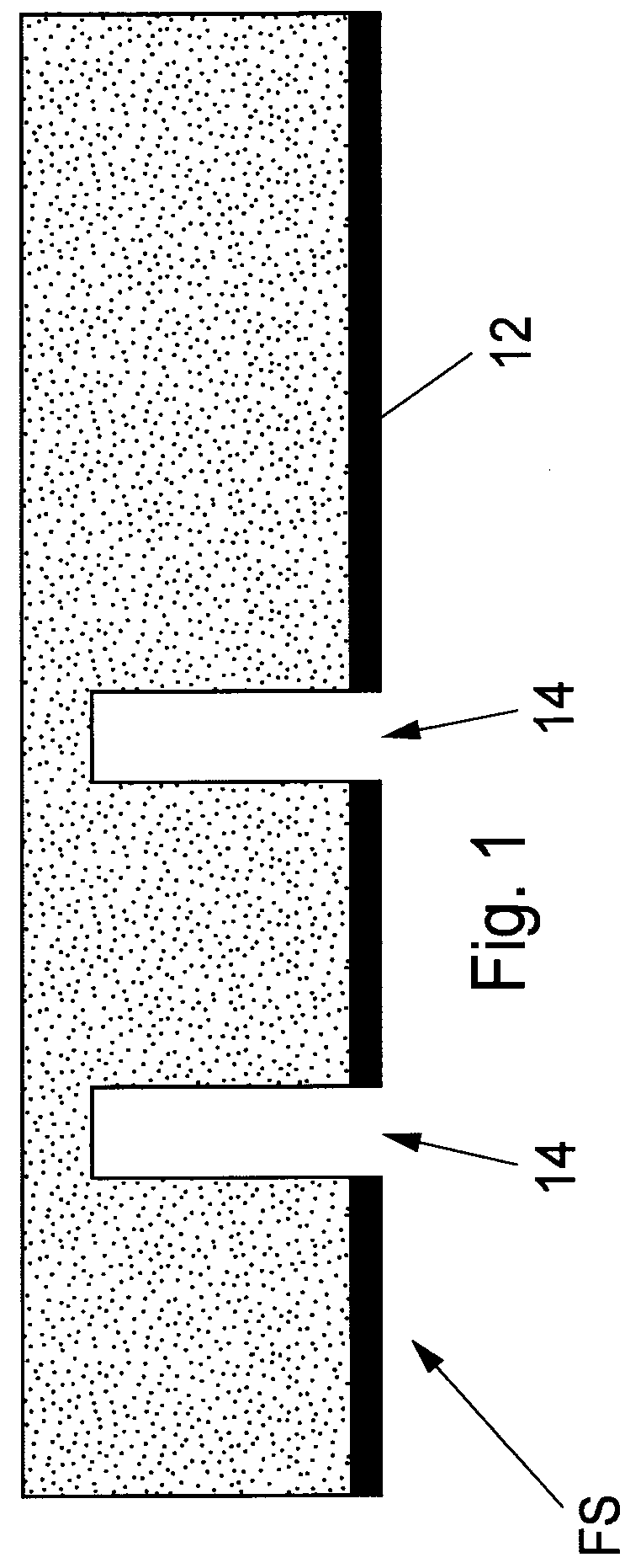
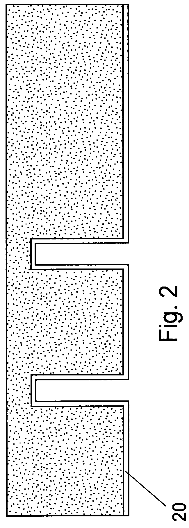
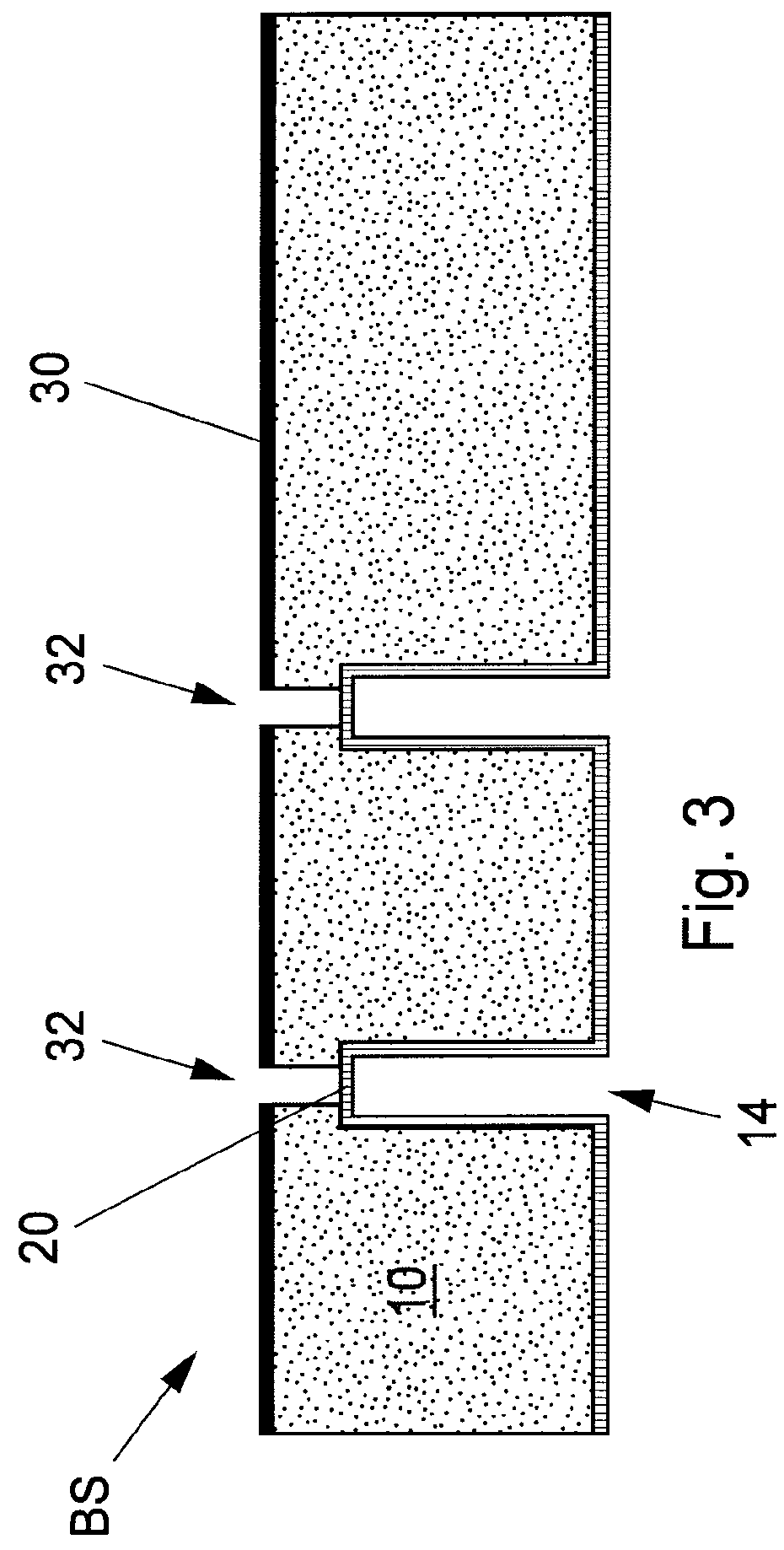
[0015]The present invention is based on the inventive concept of using a method for making a “metal via substrate”, i.e. a substrate having impedance adapted electrical through connections of metal, for RF applications, and in the same process sequence in said method optionally making a plurality of passive components, e.g. resistors, capacitors and / or inductances, said passive components extending through the substrate. Such a metal via substrate is suitable for use in hermetic capping of electronic and micro-electronic / mechanic structures in general, including but not limited to CMOS components, NMOS, PMOS, bipolar, thin or thick film passive or active devices in micro-scale and / or MEMS components such as inertial structures, gyros, accelerometers, switches in micro-scale, CMOS and / or MEMS devices, e.g. CMOS structures comprising switches.

[0016]The invention can be used to make a single transmitter / receiver chip integrated with switches and RCL filters that filters out correct fre...


PUM


Abstract

A wafer level method of making a micro-electronic and / or micro-mechanic device, having a capping with electrical wafer through connections (vias), comprising the steps of providing a first wafer of a semiconductor material having a first and a second side and a plurality of holes and / or recesses in the first side, and a barrier structure extending over the wafer on the second side, said barrier comprising an inner layer an insulating material, such as oxide, and an outer layer of another material. Then, metal is applied in said holes so as to cover the walls in the holes and the bottom of the holes. The barrier structure is removed and contacts are provided to the wafer through connections on the back-side of the wafer. Bonding structures are provided on either of said first side or the second side of the wafer. The wafer is bonded to another wafer carrying electronic and micro-electronic / mechanic components, such that the first wafer forms a capping structure covering the second wafer. Finally the wafer is singulated to individual devices.

Description

[0001]The present invention relates to packaging of semiconductor devices, and in particular to a capping substrate comprising functional features.BACKGROUND OF THE INVENTION[0002]In so called packaging of semiconductor devices it is sometimes required to enclose various components in a controlled atmosphere, i.e. to seal a cavity in a controlled atmosphere, in some cases, even most often to form a hermetic seal. This procedure entails bonding two wafers together often under pressure and with heating. This is a delicate task when wafers are thin because they easily break.[0003]Representative prior art for this field of technology are WO 2007 / 089206, WO 2008 / 091220, WO 2008 / 091221, and SE-0900590-1 (not published) all assigned to Silex Microsystems, and WO 2009 / 005462 (Nilsson et al). These documents describe various aspects of through silicon insulator technology, such as through silicon vias (TSV), “zero cross-talk” and wafer level micro-scale packaging of discrete or monolithic in...

Claims


Application Information

Patent Timeline
Patent Type & Authority Patents(United States)
IPC IPC(8): H01L21/768H01L23/66H01L23/552H01L23/58H01L23/64H01L21/683B81B7/00H01L21/50H01L21/60H01L23/48H01L23/04H01L21/78H01L23/10H01L23/00
CPCH01L21/50B81B7/007H01L21/6835H01L23/552H01L23/585H01L23/642H01L23/645H01L23/66H01L24/03H01L24/05H01L24/29H01L24/30H01L2224/81005H01L2224/81203H01L2224/81801H01L2224/83005H01L2224/83203H01L2224/83801H01L2224/83805H01L2924/014H01L2924/0105H01L2924/01005B81B2207/095H01L21/76898H01L21/78H01L23/10H01L23/481H01L24/11H01L24/13H01L24/16H01L24/27H01L24/32H01L24/33H01L24/81H01L24/83H01L2221/68363H01L2221/68372H01L2223/6616H01L2223/6622H01L2223/6655H01L2223/6677H01L2224/0239H01L2224/02311H01L2224/02313H01L2224/02371H01L2224/02372H01L2224/03462H01L2224/0401H01L2224/05073H01L2224/05155H01L2224/05548H01L2224/05573H01L2224/05644H01L2224/1146H01L2224/131H01L2224/13009H01L2224/13024H01L2224/13083H01L2224/13111H01L2224/13144H01L2224/13155H01L2224/29009H01L2224/29011H01L2224/29012H01L2224/29018H01L2224/29101H01L2224/29111H01L2224/29144H01L2224/3012H01L2224/30051H01L2924/01006H01L2924/01013H01L2924/01029H01L2924/0132H01L2924/01033H01L2924/01051H01L2924/01072H01L2924/01079H01L2924/01322H01L2924/1461H01L2924/19041H01L2924/19043H01L2924/19042H01L2924/3011H01L2924/3025H01L2924/30105H01L2924/30107H01L2924/00H01L2924/01027H01L2924/01028H01L2924/3512B81C1/00301B81C1/0023H01L21/52H01L23/04H01L23/49827H01L23/49838
Inventor EBEFORS, THORBJORNKALVESTEN, EDVARDBAUER, TOMAS
Owner SILEX MICROSYST
Why Eureka
Try Eureka