
Varnish containing good solvent and poor solvent

a solvent and solvent technology, applied in the field of varnish, can solve the problems of reducing the yield of organic el devices, reducing the reproducibility of devices, and reducing the yield of devices, and achieves the effects of reducing the occurrence of contamination particles, good reproducibility, and high levelness and uniformity

Active Publication Date: 2016-02-02
NISSAN CHEM IND LTD
View PDF64 Cites 0 Cited by
  • Summary
  • Abstract
  • Description
  • Claims
  • Application Information

AI Technical Summary

Benefits of technology

The present invention relates to a varnish for coating charge-transporting thin films used in organic EL devices. The invention aims to provide a varnish that can create thin films with high levelness, uniformity, and reduced contamination particles. The invention has been tested on contamination particles in charge-transporting thin films and shown to have significantly reduced contamination particles. The varnish is easy to prepare, can be applied using various wet processes, and can form thin films with good reproducibility. Additionally, the invention has shown that thin films with low levels of contamination particles exhibit superior electrical short-circuit prevention in organic EL devices.

Problems solved by technology

Roughness of a thin film induces the occurrence of dark spots and reductions in device characteristics due to short circuiting between an anode and a cathode.
Such roughness, therefore, becomes a cause of a reduction in yield upon fabrication of organic EL devices.
The occurrence of contamination particles also gives devices such deleterious effects as mentioned above.
The thickness of an organic layer in a general organic EL device is as small as from 200 to 1,000 nm, so that the existence of contamination articles becomes a direct cause of electric short circuiting between an anode and a cathode and is a serious problem for the device.
However, such a replacement is unable to obtain sufficient device characteristics in many instances, and requires numerous trials and errors for the selection of a material.
This problem of contamination particles is serious not only in thin films for electronic devices but also in other technical fields that use thin films.

Method used


Image

  • Varnish containing good solvent and poor solvent
  • Varnish containing good solvent and poor solvent
  • Varnish containing good solvent and poor solvent

Examples


example 1

[0152]Phenyltetraaniline (hereinafter abbreviated as “PTA”) represented by the formula (7) was synthesized from p-hydroxydiphenylamine and p-phenylenediamine in accordance with Bulletin of Chemical Society of Japan, 67, 1749-1752 (1994) (yield: 85%).

[0153][Chemical Formula 12]

[0154]

[0155]The resultant PTA (0.0500 g, 0.1130 mmol) and 5-sulfosalicylic acid (5-SSA) represented by the formula (8) (product of Wako Pure Chemical Industries, Ltd.; 0.0986 g, 0.4520 mmol)) were completely dissolved in 1,3-dimethyl-2-imidazolidinone (DMI, 5.8846 g) under a nitrogen atmosphere.

[0156][Chemical Formula 13]

[0157]

[0158]To the thus-obtained solution, cyclohexanol (c-HexOH, 8.8268 g) was added, followed by stirring to prepare a charge-transporting varnish (solid content: 1.0%).

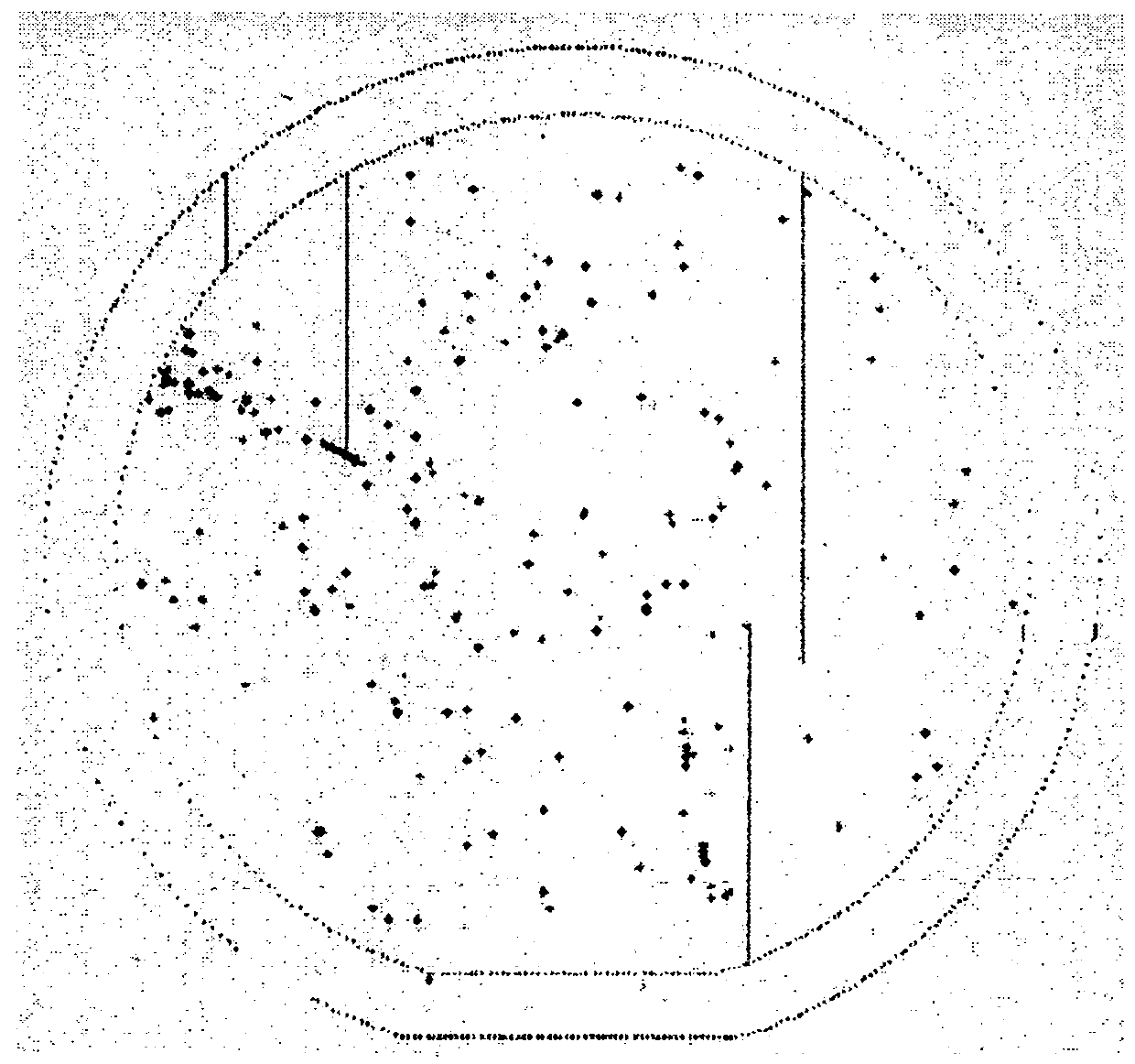
[0159]FIG. 1 illustrates the results of an inspection and measurement of surface contamination particles on a charge-transporting thin film obtained by forming a varnish of Example 1 into a film on a silicon wafer and baking t...

example 2

[0166]In a similar manner as in Example 1, PTA (0.1000 g, 0.2260 mmol) and 5-SSA (0.1972 g, 0.9040 mmol) were completely dissolved in DMI (4.1775 g) under a nitrogen atmosphere.

[0167]To the thus-obtained solution, c-HexOH (6.2662 g) was added, followed by stirring to prepare a charge-transporting varnish (solid content: 3.0%).

example 3

[0168]In a similar manner as in Example 1, PTA (0.1000 g, 0.2260 mmol) and 5-SSA (0.1972 g, 0.9040 mmol) were completely dissolved in N-methylpyrrolidone (4.1775 g) under a nitrogen atmosphere.

[0169]To the thus-obtained solution, c-HexOH (6.2662 g) was added, followed by stirring to prepare a charge-transporting varnish (solid content: 3.0%).


PUM

PropertyMeasurementUnit
boiling pointaaaaaaaaaa
thicknessaaaaaaaaaa
thicknessaaaaaaaaaa

Abstract

A varnish comprising a ground substance consisting of a polymer or oligomer of 200 to 50′104 molecular weight or organic compound of 200 to 1000 molecular weight and a solvent containing a good solvent and a poor solvent whose boiling point (under 760 mmHg) is at least 20° C. lower than that of the good solvent, wherein the ground substance is dissolved in the solvent. Any thin film prepared from this varnish is substantially from generation of foreign matter, so that it can appropriately be used as thin films for electronic devices and those for use in other technical fields.

Description

TECHNICAL FIELD[0001]This invention relates to a varnish including a good solvent and a poor solvent.BACKGROUND ART[0002]When an organic compound, especially a polymer or oligomer is used as an electronic device material, it is often used as thin films. Illustrative are insulating films, charge-transporting films, protecting films, and leveling films.[0003]In organic electroluminescence (hereinafter abbreviated as “EL”) devices, charge-transporting thin films made of a polymer or oligomer or the like are used as hole transport layers (buffer layers) and / or charge injection layers (see, for example, Patent Document 1).[0004]A charge-transporting thin film is required to be a uniform, roughness-free thin film. Roughness of a thin film induces the occurrence of dark spots and reductions in device characteristics due to short circuiting between an anode and a cathode. Such roughness, therefore, becomes a cause of a reduction in yield upon fabrication of organic EL devices. This roughnes...

Claims


Application Information

Patent Timeline
Patent Type & Authority Patents(United States)
IPC IPC(8): C08G73/00H01L51/00C09D179/06C09D179/04C09D179/02C09D165/00C08G73/22H01B1/12C08G73/02C08G73/08C08G73/18H01L51/50H05B33/10H05B33/14H05B33/22H10K99/00
CPCH01B1/122C08G73/0266C08G73/08C08G73/18C08G73/22C09D165/00C09D179/02C09D179/04C09D179/06H01L51/0007H01L51/5052H10K71/15H10K50/155C09K11/06
Inventor KATO, TAKUYOSHIMOTO, TAKUJIONO, GO
Owner NISSAN CHEM IND LTD
Learn More