High voltage metal-oxide-semiconductor transistor device

a technology of metal-oxide-semiconductor and transistor, which is applied in the direction of semiconductor devices, basic electric elements, electrical equipment, etc., can solve the problems of reducing esd damage, breaking down voltage and ron, etc., and achieves the effect of improving the reliability of hv mos and reducing current flow through the source region

Active Publication Date: 2015-12-29
UNITED MICROELECTRONICS CORP
View PDF7 Cites 5 Cited by
  • Summary
  • Abstract
  • Description
  • Claims
  • Application Information

AI Technical Summary

Benefits of technology

[0008]Compared with conventional HV MOS, the source region of the HV MOS of the present invention is composed of two parts with different conductivity types. More precisely, the source region of the present invention comprises the first part and the second part, and the first part and the second part have complementary conductivity types. Therefore, since the high voltage current that is transmitted from the drain region to the source region is dispersed, the current flow passing through the source region can be decreased, thereby avoiding the ESD damage happened and improving the reliability of the HV MOS.

Problems solved by technology

However, breakdown voltage and RON are conflicting parameters with a trade-off relationship.
In addition, the electrostatic discharge (ESD) may also influence the performance of a LDMOS, so decreasing the ESD damage of a LDMOS is an important issue for researching.

Method used


Image

  • High voltage metal-oxide-semiconductor transistor device
  • High voltage metal-oxide-semiconductor transistor device
  • High voltage metal-oxide-semiconductor transistor device

Examples


Embodiment Construction

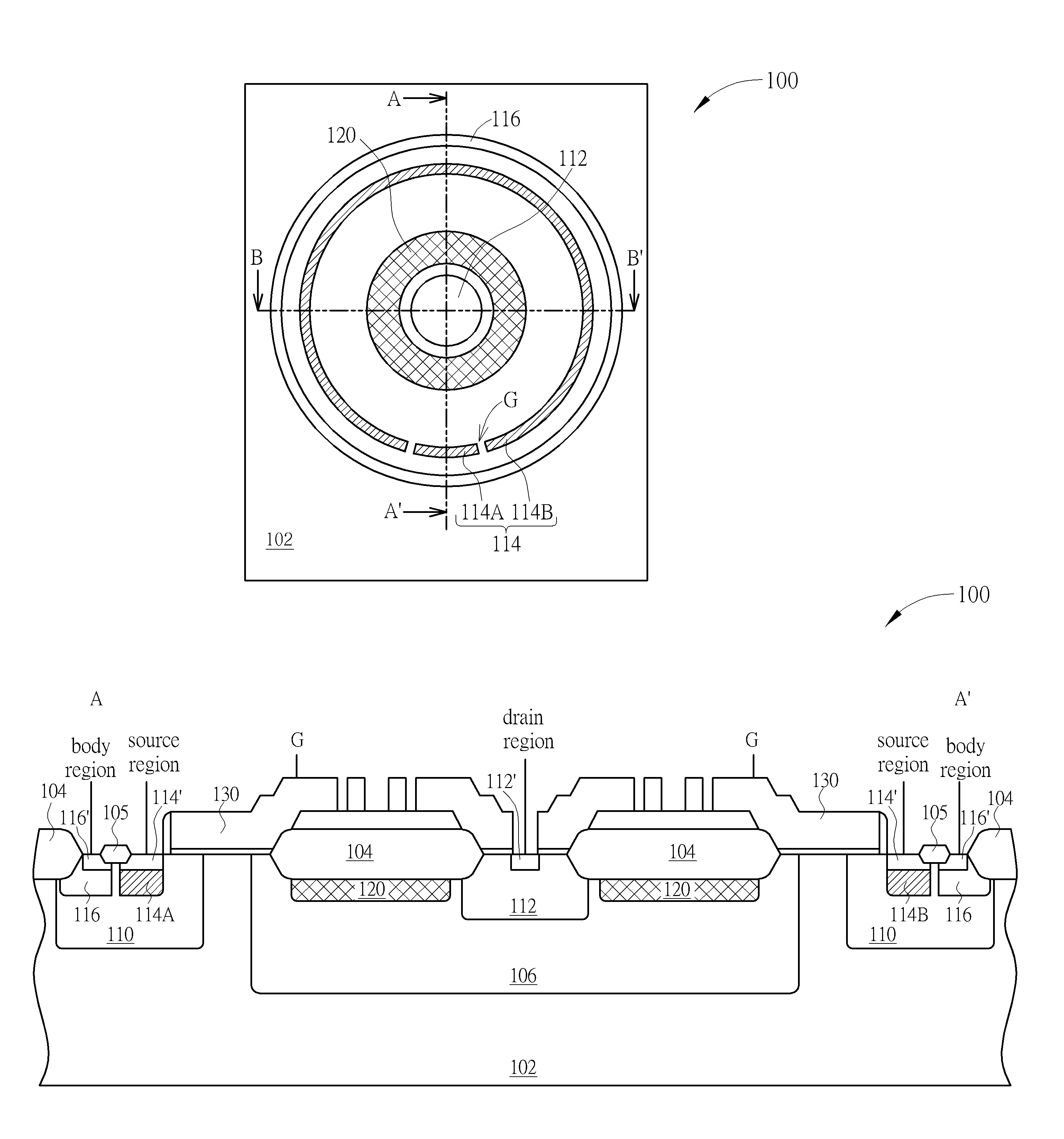
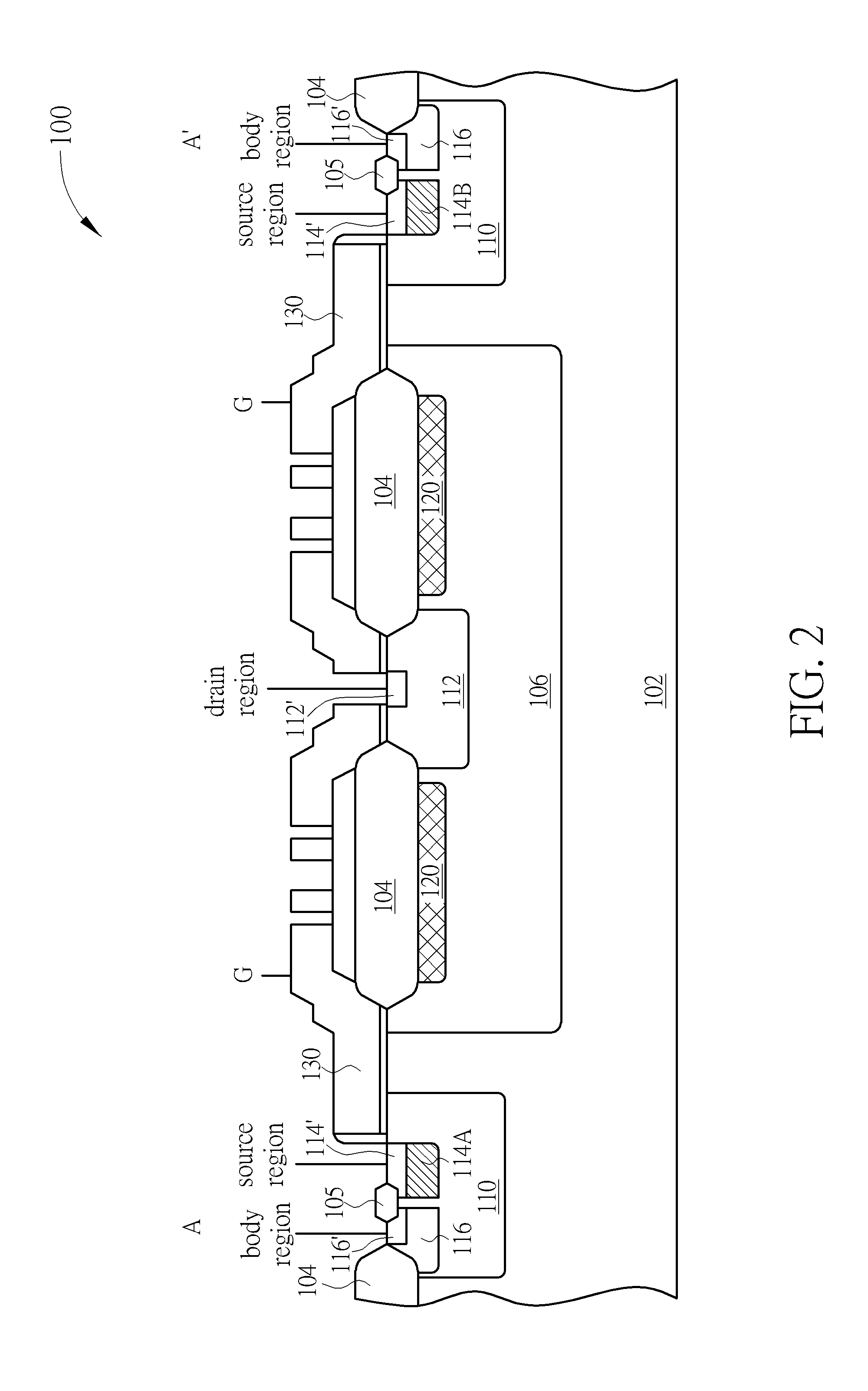
[0014]Please refer to FIGS. 1-3, FIG. 1 is a schematic drawing of a layout pattern of a HV MOS transistor device provided by a first preferred embodiment of the present invention, FIG. 2 is a cross-sectional view of the HV MOS transistor device provided by the first preferred embodiment taken along line A-A′ of FIG. 1; FIG. 3 is a cross-sectional view of the HV MOS transistor device provided by the first preferred embodiment taken along line B-B′ of FIG. 1. As shown in FIGS. 1-3, a HV MOS transistor device 100 provided by the preferred embodiment is positioned in a substrate 102, such as a silicon substrate. The substrate 102 includes a first conductivity type. In the preferred embodiment, the first conductivity type is p type. The HV MOS transistor device 100 further includes an insulating layer 104, such as a filed oxide (FOX) or a shallow trench isolation (STI). It is noteworthy that for clarifying spatial relationships between certain specific doped regions of the HV MOS transis...


PUM


Abstract

A high voltage metal-oxide-semiconductor (HV MOS) device includes a substrate including a first conductivity type, a gate positioned on the substrate, a drain region formed in the substrate, the drain region including a second conductivity type, and a source region formed in the substrate, where the source region includes at least one first part and at least one second part, the first part includes the second conductivity type, the second part includes the first conductivity type, and the first conductivity type and the second conductivity type are complementary.

Description

BACKGROUND OF THE INVENTION[0001]1. Field of the Invention[0002]The invention relates to a high voltage metal-oxide-semiconductor (herein after abbreviated as HV MOS) device, and more particularly, to a high voltage lateral double-diffused metal-oxide-semiconductor (HV-LDMOS) device.[0003]2. Description of the Prior Art[0004]Double-diffused MOS (DMOS) transistor devices have drawn much attention in power devices having high voltage capability. The conventional DMOS transistor devices are categorized into vertical double-diffused MOS (VDMOS) transistor device and lateral double-diffused MOS (LDMOS) transistor device. Having advantages of higher operational bandwidth, higher operational efficiency, and convenience to be integrated with other integrated circuit due to its planar structure, LDMOS transistor devices are prevalently used in high operational voltage environments such as CPU power supply, power management system, AC / DC converter, and high-power or high frequency (HF) band p...

Claims


Application Information

Patent Timeline
Patent Type & Authority Patents(United States)
IPC IPC(8): H01L29/78H01L29/417H01L29/772H01L29/10H01L29/08
CPCH01L29/7816H01L29/0886H01L29/0869H01L29/1095H01L29/7835H01L29/0619H01L29/0696H01L29/063H01L29/0653H01L29/0847H01L29/1045
Inventor PU, SHIH-CHIEHLEE, MING-TSUNGYANG, CHENG-HUALI, NIEN-CHUNGLEE, WEN-FANGWANG, CHIH-CHUNG
Owner UNITED MICROELECTRONICS CORP
Why Eureka
Try Eureka