Semiconductor device
a semiconductor device and threshold voltage technology, applied in the direction of semiconductor devices, electrical equipment, transistors, etc., can solve the problems of reducing reliability and electrical characteristics, and achieve the effect of suppressing the formation of trap states, reducing reliability, and effectively controlling the threshold voltage of semiconductor devices
- Summary
- Abstract
- Description
- Claims
- Application Information
AI Technical Summary
Benefits of technology
Problems solved by technology
Method used
Image


Examples
embodiment 1
[0056]In this embodiment, one embodiment of a semiconductor device and a method for manufacturing the semiconductor device will be described with reference to FIGS. 1A to 1C, FIGS. 2A to 2C, FIGS. 3A to 3C, and FIGS. 4A to 4C. In this embodiment, a transistor including an oxide semiconductor is shown as an example of the semiconductor device.
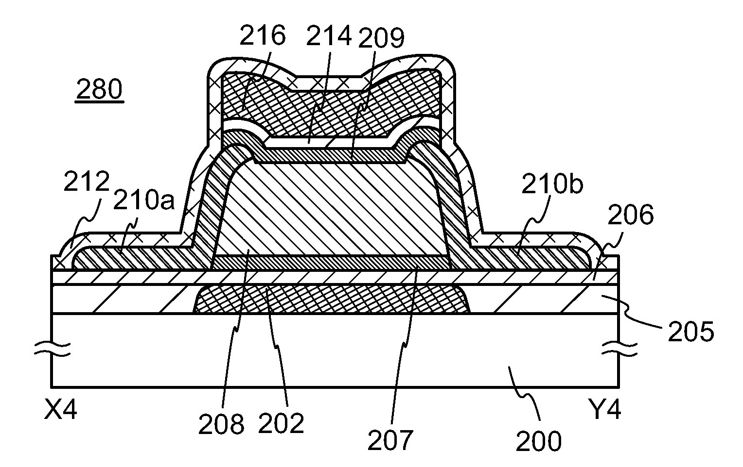
[0057]FIGS. 1A to 1C illustrate an example of a structure of a transistor 250. FIG. 1A is a plan view of the transistor 250, FIG. 1B is a cross-sectional view taken along line V1-W1 in FIG. 1A, and FIG. 1C is a cross-sectional view taken along line X1-Y1 in FIG. 1A. Note that in FIG. 1A, some components of the transistor 250 (e.g., an insulating layer 212) are not illustrated to avoid complexity. The same applies to the other plan views in this specification.
[0058]The transistor 250 illustrated in FIGS. 1A to 1C includes a first gate electrode layer 202 over a substrate 200; an insulating layer 206 in contact with the first gate electrode layer ...
embodiment 2
[0125]In this embodiment, a structure of the semiconductor device different from that in Embodiment 1 will be described with reference to FIGS. 5A to 5D and FIGS. 6A to 6C. For the components similar to those in Embodiment 1, the description of Embodiment 1 can be referred to and is not repeated in some cases.
[0126]FIGS. 5A to 5D illustrate an example of a structure of a transistor 270. FIG. 5A is a plan view of the transistor 270, FIG. 5B is a cross-sectional view taken along line V3-W3 in FIG. 5A, and FIG. 5C is a cross-sectional view taken along line X3-Y3 in FIG. 5A. FIG. 5D is a band diagram schematically showing the energy at the bottom of the conduction band of a layered structure included in the transistor 270.
[0127]The transistor 270 illustrated in FIGS. 5A to 5C includes, like the transistor 260 in Embodiment 1, the insulating layer 205 over the substrate 200; the first gate electrode layer 202 which is buried in the insulating layer 205 and has an exposed top surface; the...
embodiment 3
[0173]Described in this embodiment is an example of an oxide semiconductor layer that can be applied to the transistors of Embodiment 1 or 2.
[0174]An oxide semiconductor layer is classified roughly into a non-single-crystal oxide semiconductor layer and a single crystal oxide semiconductor layer. The non-single-crystal oxide semiconductor layer includes a c-axis aligned crystalline oxide semiconductor (CAAC-OS) layer, a polycrystalline oxide semiconductor layer, a microcrystalline oxide semiconductor layer, an amorphous oxide semiconductor layer, and the like.
[0175]First, a CAAC-OS film is described.
[0176]The CAAC-OS film is one of oxide semiconductor layers including a plurality of c-axis aligned crystal parts
[0177]In a transmission electron microscope (TEM) image of the CAAC-OS film, it is difficult to clearly observe a boundary between crystal parts, that is, a grain boundary. Thus, in the CAAC-OS film, a reduction in electron mobility due to the grain boundary is less likely to ...
PUM
 Abstract
Description
Claims
Application Information
 - R&D
- Intellectual Property
- Life Sciences
- Materials
- Tech Scout
- Unparalleled Data Quality
- Higher Quality Content
- 60% Fewer Hallucinations
Browse by: Latest US Patents, China's latest patents, Technical Efficacy Thesaurus, Application Domain, Technology Topic, Popular Technical Reports.
© 2025 PatSnap. All rights reserved.Legal|Privacy policy|Modern Slavery Act Transparency Statement|Sitemap|About US| Contact US: help@patsnap.com