
Substrate processing apparatus, method of manufacturing semiconductor device and non-transitory computer-readable recording medium

a processing apparatus and semiconductor technology, applied in the direction of coatings, chemical vapor deposition coatings, electric discharge tubes, etc., can solve the problems of difficult uniform etching or processing of substrates, difficult to form fine semiconductor devices, and difficult to improve manufacturing throughput, etc., to achieve the effect of improving manufacturing throughpu

Active Publication Date: 2015-10-27
KOKUSA ELECTRIC CO LTD
View PDF22 Cites 4 Cited by
  • Summary
  • Abstract
  • Description
  • Claims
  • Application Information

AI Technical Summary

Benefits of technology

The present invention is a substrate processing apparatus that can create films with different thicknesses and features on a substrate. This improves the manufacturing process and increases production efficiency. The invention also provides a method for making a semiconductor device, and a computer-readable recording medium that is used for this purpose.

Problems solved by technology

Recently, as a circuit pattern becomes finer, filling a fine structure and particularly, filling a structure having a gap (groove), which is deep in the vertical direction or that is narrow in the horizontal direction, with an oxide by chemical vapor deposition (CVD) has become technically limited.
Also, it has been difficult to uniformly etch or process a substrate having a groove that is deep in the vertical direction by chemical mechanical polishing (CMP).
Thus, it has become difficult to form a fine semiconductor device, improve the manufacturing throughput, or uniformly process a substrate while maintaining the quality thereof constant.

Method used


Image

  • Substrate processing apparatus, method of manufacturing semiconductor device and non-transitory computer-readable recording medium
  • Substrate processing apparatus, method of manufacturing semiconductor device and non-transitory computer-readable recording medium
  • Substrate processing apparatus, method of manufacturing semiconductor device and non-transitory computer-readable recording medium

Examples


first embodiment

[0028]A first embodiment of the present invention will be described with reference to the accompanying drawings below.

Structure of Substrate Processing Apparatus

[0029]First, a substrate processing apparatus 100 according to the first embodiment will be described.

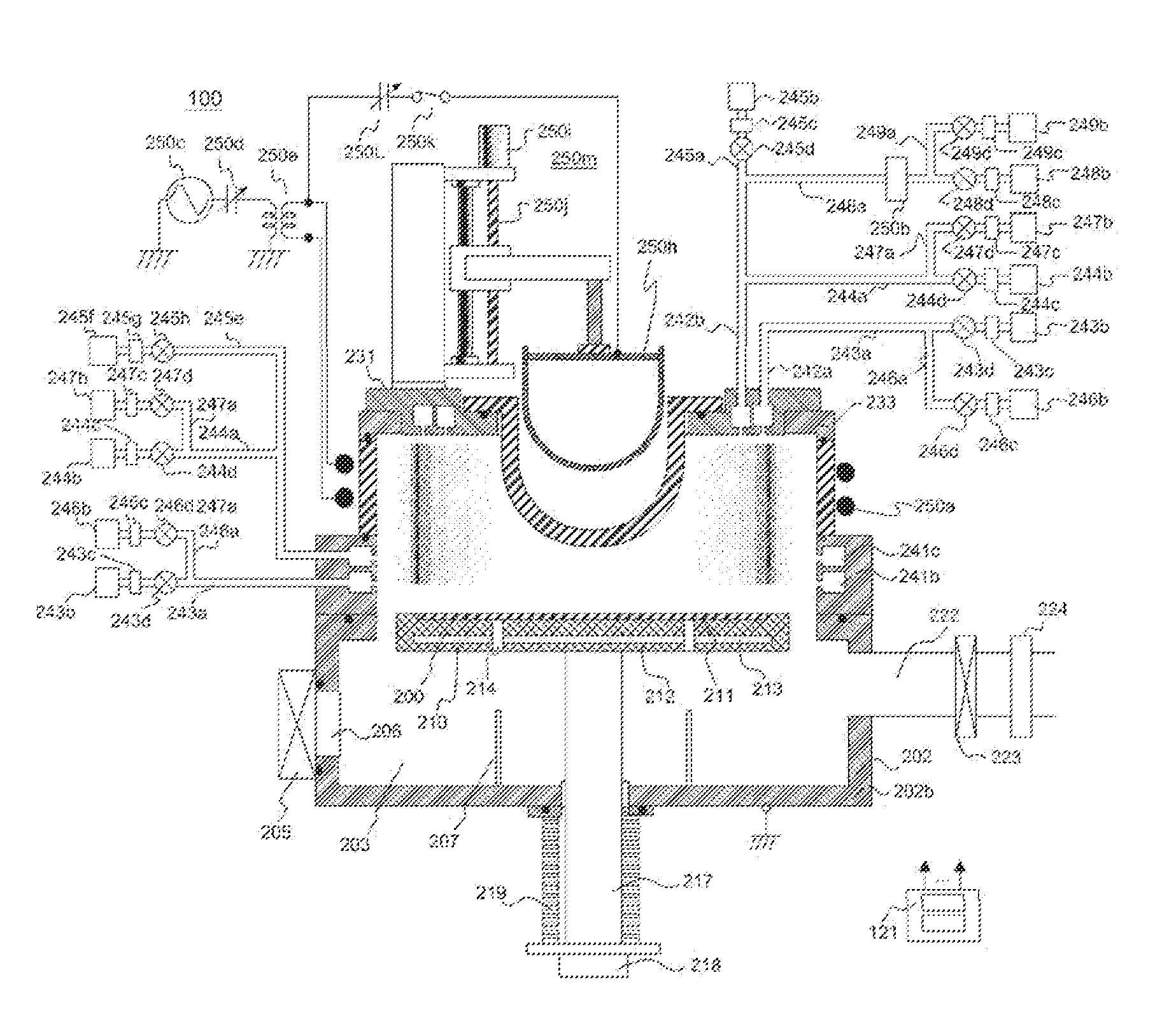
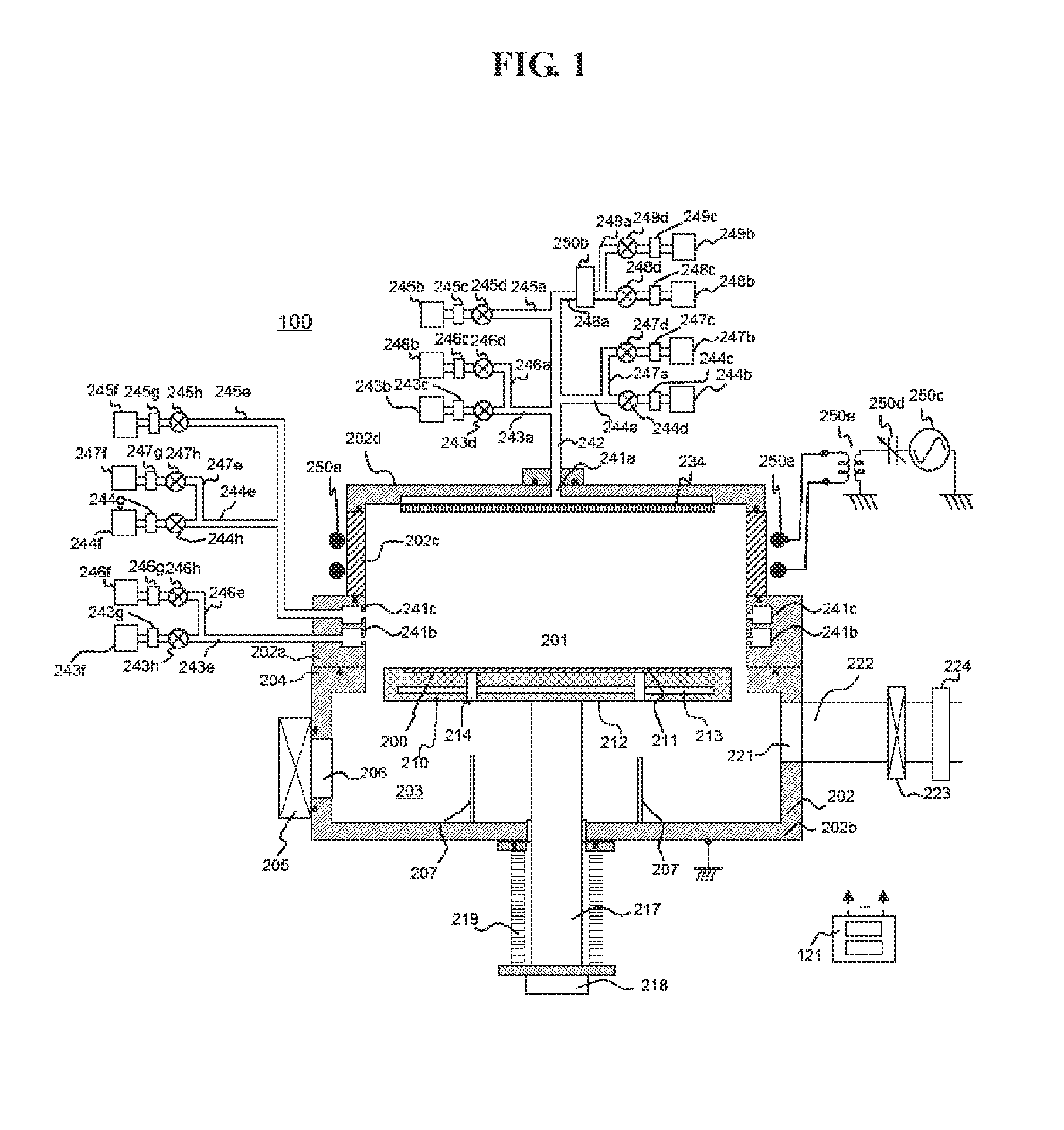
[0030]The substrate processing apparatus 100 according to the present embodiment will now be described. The substrate processing apparatus 100 is a unit configured to form an insulating film, a metal film, or the like and is configured as a single-wafer type substrate processing apparatus as illustrated in FIG. 1.

[0031]Referring to FIG. 1, the substrate processing apparatus 100 includes a process container 202. The process container 202 is configured, for example, as an airtight container having a flat cylindrical circular cross-section. Also, the process container 202 is formed, for example, of a metal material, e.g., aluminum (Al) or stainless steel (steel-use-stainless (SUS)) or quartz. In the process container 202, a pro...

second embodiment

[0128]Although the first embodiment has been described above in detail, the present invention is not limited thereto and may be embodied in various forms without departing from the scope of the invention. For example, an embodiment of FIG. 9 may be accomplished.

[0129]Referring to FIG. 9, a coil 250a is configured to be upwardly / downwardly movable. The coil 250a may be moved upward / downward by moving an elevator 250g upward / downward by connecting the coil 250a and a matching box 250f to the elevator 250g.

[0130]For example, when the coil 250a is moved upward in a state in which predetermined conditions of supplying a first reactive gas and a second reactive gas are set, the efficiency of processing the center portion of the wafer 200 is greater than the efficiency of processing the peripheral portion of the wafer 200 and thus the thickness of the film on the center portion of the wafer 200 increases, thereby forming a film having the film thickness distribution A of FIG. 5. When the ...

third embodiment

[0132]Although the second embodiment has been described above in detail, the present invention is not limited thereto and may be embodied in various forms without departing from the scope of the invention.

[0133]The inventors of the present invention have found that since plasma was concentrated near an outer circumference of the processing chamber 201 (the coil 250a) in a plasma device using a coil as described above, the peripheral portion of the wafer 200 was easily processed to cause a film to be thickly formed on the peripheral portion compared to the center portion of the wafer 200, and the quality of the film was likely to be changed to make it difficult to control the center portion of the wafer 200. The quality of the film may be determined by, for example, permittivity, resistivity, etc. Thus, the inventors have conducted a study and found that a center portion of a substrate can be easily controlled by adjusting a distribution of plasma using a structure as illustrated in ...


PUM

PropertyMeasurementUnit
widthaaaaaaaaaa
pressureaaaaaaaaaa
temperatureaaaaaaaaaa

Abstract

A substrate processing apparatus includes a processing chamber accommodating a substrate; first and second process gas supply units that respectively supply first and second process gases from above and laterally relative to the substrate; and first and second reactive gas supply units that respectively supply first and second reactive gases from above and laterally relative to the substrate. A control unit controls the other units such that a total amount of the first and second process gases supplied to a center portion of the substrate is different from that supplied to a peripheral portion of the substrate, or a total amount of the first and second reactive gases supplied to the center portion of the substrate is different from that supplied to the peripheral portion of the substrate.

Description

CROSS-REFERENCE TO RELATED PATENT APPLICATION[0001]This application claims foreign priority under 35 U.S.C. §119(a)-(d) to Application No. JP 2014-170371 filed on Aug. 25, 2014, entitled “Substrate Processing Apparatus, Method of Manufacturing Semiconductor Device and Non-Transitory Computer Readable Recording Medium,” the entire contents of which are hereby incorporated by reference.FIELD OF THE INVENTION[0002]The present invention relates to a substrate processing apparatus, a method of manufacturing a semiconductor device and a non-transitory computer readable recording medium.DESCRIPTION OF THE RELATED ART[0003]As the integration degree of a large-scale integrated circuit (hereinafter referred to as “LSI”) becomes higher, a circuit pattern becomes finer.[0004]A device should be formed in a small size to accommodate a large number of semiconductor devices in a narrow area. To this end, the widths of and distances between patterns that are to be formed should be set to be small.[0...

Claims


Application Information

Patent Timeline
Patent Type & Authority Patents(United States)
IPC IPC(8): C23F1/00H01L21/3065H01L21/02H01J37/32C23C16/455C23C16/52C23C16/50H01L21/67
CPCH01L21/3065H01L21/0262H01L21/67069C23C16/50C23C16/52C23C16/45523C23C16/45502H01J37/3244H01L21/67017H01L21/68742H01L21/68792C23C16/345C23C16/455C23C16/45563C23C16/507H01J37/321H01J37/32697H01J37/32926H01L21/0217H01L21/02211H01L21/02274H01L21/0228
Inventor TOYODA, KAZUYUKIMATSUI, SHUN
Owner KOKUSA ELECTRIC CO LTD
Learn More