Eureka AIR delivers breakthrough ideas for toughest innovation challenges, trusted by R&D personnel around the world.

Semiconductor apparatus comprised of two types of transistors

a technology of semiconductor materials and semiconductor devices, applied in the direction of amplifiers with field-effect devices, semiconductor/solid-state device details, solid-state devices, etc., can solve the problems of poor linearity of semiconductor materials primarily based on nitride, and achieve the effect of poor linearity and simple arrangement and process

Active Publication Date: 2015-10-06
SUMITOMO ELECTRIC IND LTD
View PDF7 Cites 0 Cited by
  • Summary
  • Abstract
  • Description
  • Claims
  • Application Information

AI Technical Summary

Benefits of technology

[0008]Because the first semiconductor chip is separated from the second semiconductor chip, the first semiconductor chip may implement the first transistor independent of the second transistor. The second transistor may be based on nitride based materials, such as GaN, AlGaN, and so on. However, a transistor primarily based on nitride semiconductor materials shows a poor linearity in spite of the voltage endurance thereof. Embodiments of the present application may provide one of solutions to compensate this degraded linearity of the nitride transistor by introducing another type of transistor, namely, a transistor made of GaAs based material by a simple arrangement and process.

Problems solved by technology

However, a transistor primarily based on nitride semiconductor materials shows a poor linearity in spite of the voltage endurance thereof.

Method used


Image

  • Semiconductor apparatus comprised of two types of transistors
  • Semiconductor apparatus comprised of two types of transistors
  • Semiconductor apparatus comprised of two types of transistors

Examples


first embodiment

[0024

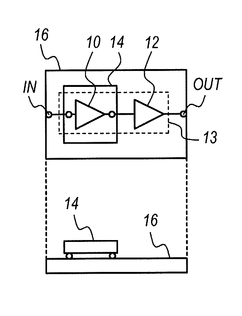
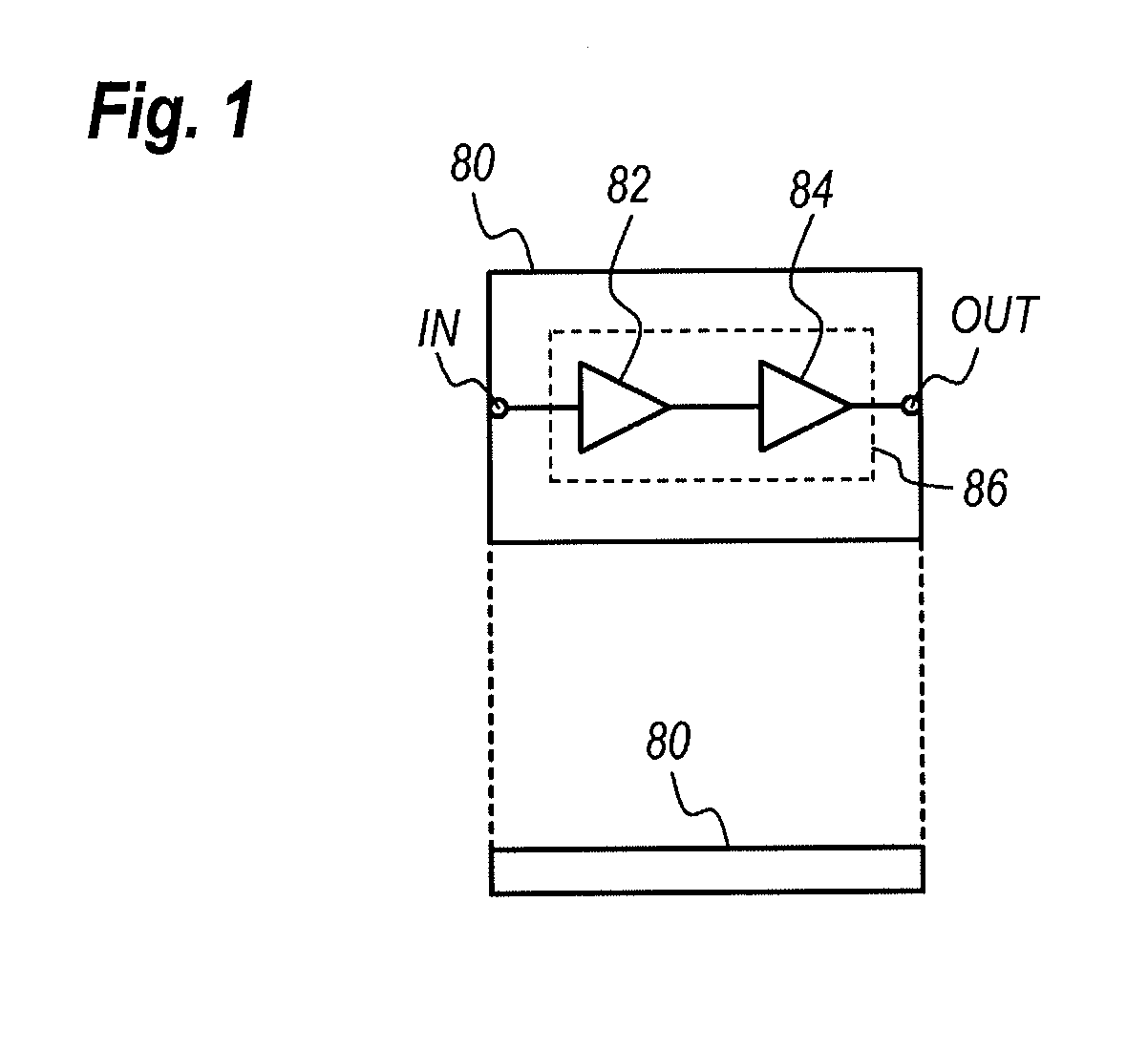
[0025]FIG. 3 schematically illustrates a semiconductor apparatus according to an embodiment of the invention, where the semiconductor apparatus is a type of a power amplifier 13. The power amplifier 13 has a configuration that two transistors, 10 and 12, are sequentially arranged between the input IN and the output OUT, like those of the comparable example shown in FIG. 1 but the first transistor 10 is formed on the first semiconductor chip 14, and this first semiconductor chip 14 is mounted on the second semiconductor chip 16 where the second transistor 12 is formed. As described later in the specification, the first transistor 10 is a type of a GaAs-HEMT; while, the second transistor 12 is a type of a GaN-HEMT formed on the SiC substrate. The first semiconductor chip 14 is mounted on an inactive region of the second semiconductor chip 16.

[0026]Because the first semiconductor chip 14 is mounted on the second semiconductor chip 16 accompanied with, for instance, bump electrodes...

second embodiment

[0040](Second Embodiment)

[0041]The semiconductor apparatus according to the first embodiment of the invention shown in FIG. 3 has an arrangement of the flip-chip boding for the first semiconductor chip 14, where the first semiconductor chip 14 faces the primary surface thereof down to the second semiconductor chip 16. However, the arrangement for the first semiconductor chip 14 is not restricted to those of what we call face-down assembly. A face-up assembly accompanied with ordinary wire bonding is applicable to the semiconductor apparatus. FIGS. 8A to 8E show processes to form such semiconductor apparatus with face-up assembly.

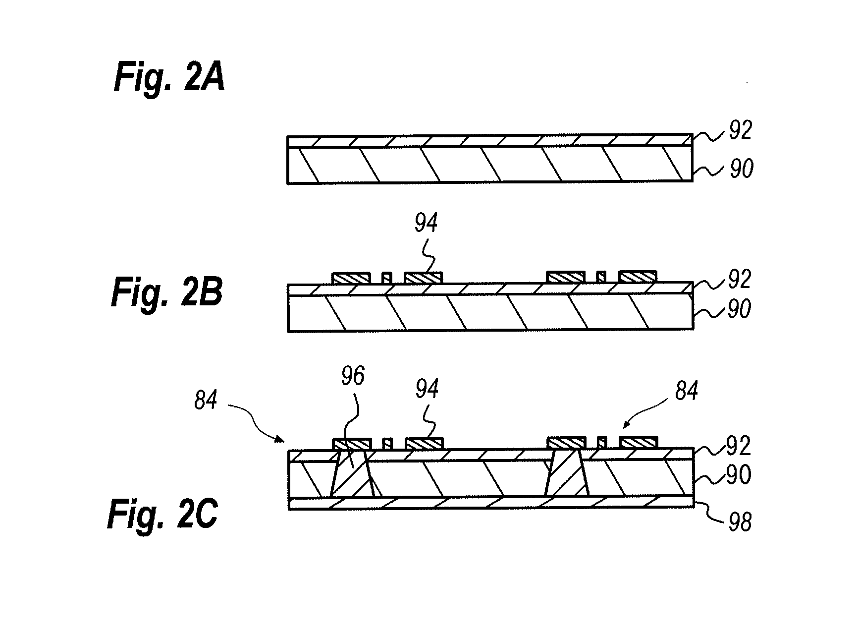
[0042]An epitaxial layer 32 is first grown on the substrate 30 (FIG.8A). Removing a portion of the epitaxial layer 32 (FIG. 8B), metal electrodes 34 and interconnections 31 are formed on the left epitaxial layer 32 and the exposed surface of the substrate 30 (FIG. 8C). The left epitaxial layer 32 and the electrodes 34a, constitute the second transistor 12 of...

third embodiment

[0045

[0046]FIGS. 9A to 9C are schematic plan views of semiconductor apparatuses according to the third embodiment of the invention, where the semiconductor apparatuses each include a power amplifier with an arrangement of two arms connected in parallel to each other between input IN and output OUT terminals, and each of arms has three (3) stages. Three transistors in the respective arms are connected in series. Specifically, the three-stage amplifier includes three transistors, T1, to T3, and T4, to T6, connected in series. Transistors involved in the semiconductor chip 14 mounted on the inactive area of the second semiconductor chip 16, namely, transistors, T1and T4, in FIG. 9A, transistors, T1, T2, T4, and T5, in FIG. 9B, and transistors, T1, and T4, and T2, and T5, in FIG. 9C have the type, GaAs-HEMT. On the other hand, other transistors not involved in the first semiconductor chip 14 have the type, GaN-HEMT formed on the second semiconductor chip 16.

[0047]Describing further spec...


PUM


Abstract

A semiconductor apparatus that includes two types of transistors is disclosed. A first semiconductor chip includes the first semiconductor device of a transistor type of GaAs-HEMT, while, a second semiconductor chip includes a second semiconductor device of a transistor type GaN-HEMT. The second semiconductor device is formed on a SiC substrate, and the first semiconductor chip is mounted in an inactive region of the SiC substrate.

Description

BACKGROUND OF THE INVENTION[0001]1. Field of the Invention[0002]The present application relates to a semiconductor apparatus, in particular, the application relates to a power amplifier including semiconductor devices.[0003]2. Related Background Arts[0004]A power amplifier including a plurality of transistors each connected in series has been well known in the field. A multi-stage architecture of the semiconductor transistors is preferable to obtain a desirable gain. A Japanese patent application published as JP-H06-232661A has disclosed such a multi-stage power amplifier.[0005]Recently, nitride semiconductor materials such as GaN, AlGaN, and so on, have been attracted because of their excellent voltage endurance. However, nitride based transistors show linearity insufficient for some applications. For instance, a multi-stage power amplifier constituted by nitride based transistors show far insufficient linearity.[0006]On the other hand, transistors primarily comprised of GaAs based...

Claims


Application Information

Patent Timeline
Patent Type & Authority Patents(United States)
IPC IPC(8): H03F3/16H01L29/66H01L29/778H01L29/20H01L27/06H01L25/00H03F3/21H03F1/02H03F3/193H03F3/24H01L25/065H01L25/18H01L27/085H01L21/8252H01L23/00
CPCH01L27/0605H01L25/0652H01L25/0657H01L25/18H01L25/50H01L29/2003H01L29/66462H01L29/7783H01L29/7787H03F1/0272H03F3/193H03F3/21H03F3/211H03F3/24H01L21/8252H01L24/05H01L24/06H01L24/13H01L24/16H01L27/085H01L2224/0401H01L2224/04042H01L2224/0557H01L2224/06181H01L2224/131H01L2224/16145H01L2224/48091H01L2224/48145H01L2224/73265H01L2225/06506H01L2225/06513H01L2225/06541H01L2225/06568H01L2225/06589H01L2924/00014H01L2924/1033H01L2924/10253H01L2924/10272H01L2924/10329H01L2924/10336H01L2924/10337H01L2924/10344H01L2924/12032H01L2924/1306H01L2924/13052H01L2924/13064H03F2200/408H03F2200/411H01L2924/014H01L2224/05552H01L2924/00H01L2924/00012
Inventor YAMADA, FUMIO
Owner SUMITOMO ELECTRIC IND LTD
Why Eureka
Eureka Blog
Learn More