Interconnect substrate with embedded semiconductor device and built-in stopper and method of making the same

a technology of interconnect substrate and semiconductor device, which is applied in the direction of semiconductor device, semiconductor/solid-state device details, thin material processing, etc., can solve the problems of inability to accurately the failure of the embedding chip in the wiring board, and the inability to offer a proper solution or effective method for controlling the movement of the die, etc., to achieve high i/o and high performance, accurate confine the placement location of the semiconductor device, and the effect of high-quality

Inactive Publication Date: 2015-09-29
BRIDGE SEMICON
View PDF14 Cites 0 Cited by
  • Summary
  • Abstract
  • Description
  • Claims
  • Application Information

AI Technical Summary

Benefits of technology

The present invention provides an interconnect substrate with dual build-up circuitries that securely retains electrical connection between a semiconductor device and the build-up circuitry, while avoiding the problem of lateral displacement of the semiconductor device. The direct electrical connection between the semiconductor device and the build-up circuitry without solder is advantageous for high I / O and high performance. Additionally, the interconnect substrate made by this method is reliable, inexpensive, and well-suited for high volume manufacture.

Problems solved by technology

However, the attempt of embedding chip in a wiring board can encounter many problems.
The CTE mismatch between metal, dielectric and silicon at various stages of thermal treatment can result in misalignment of the build-up interconnect structure to be deposited thereon.
None of these approaches offers a proper solution or effective method for controlling die movement because the underneath adhesive will reflow during curing and therefore dislocates the attached die from the pre-determined location even a highly precise alignment mark and equipment are applied.
This approach may be effective in controlling die from further movement during sealing process, it does not provide any control or adjustment for die attach process and the mis-registration is unavoidable due to die attach adhesive reflows.

Method used


Image

  • Interconnect substrate with embedded semiconductor device and built-in stopper and method of making the same
  • Interconnect substrate with embedded semiconductor device and built-in stopper and method of making the same
  • Interconnect substrate with embedded semiconductor device and built-in stopper and method of making the same

Examples


embodiment 1

[Embodiment 1]

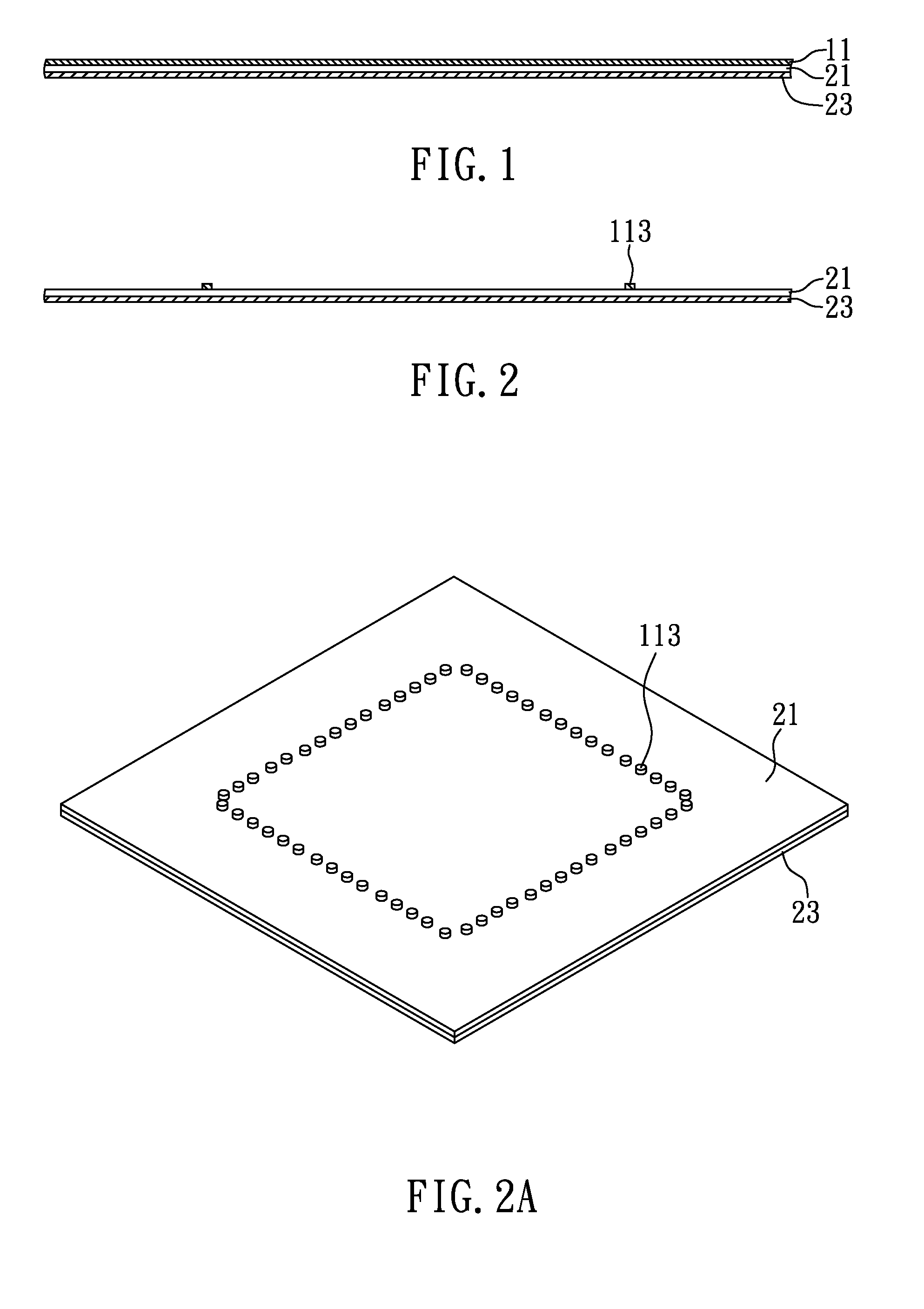
[0044]FIGS. 1 and 2 are cross-sectional views showing a method of forming a stopper on a dielectric layer in accordance with an embodiment of the present invention, and FIG. 2A is a top view corresponding to FIG. 2.

[0045]FIG. 1 is a cross-sectional view of a laminate substrate that includes metal layer 11, dielectric layer 21 and support plate 23. Metal layer 11 is illustrated as a copper layer with a thickness of 35 microns. However, metal layer 11 can also be made of other various metal materials and is not limited to a copper layer. Besides, metal layer 11 can be deposited on dielectric layer 21 by numerous techniques including lamination, electroplating, electroless plating, evaporating, sputtering, and their combinations as a single layer or multiple layers, and preferably has a thickness in a range of 10 to 200 microns.

[0046]Dielectric layer 21 typically is made of epoxy resin, glass-epoxy, polyimide and the like and has a thickness of 50 microns. In this embodim...

embodiment 2

[Embodiment 2]

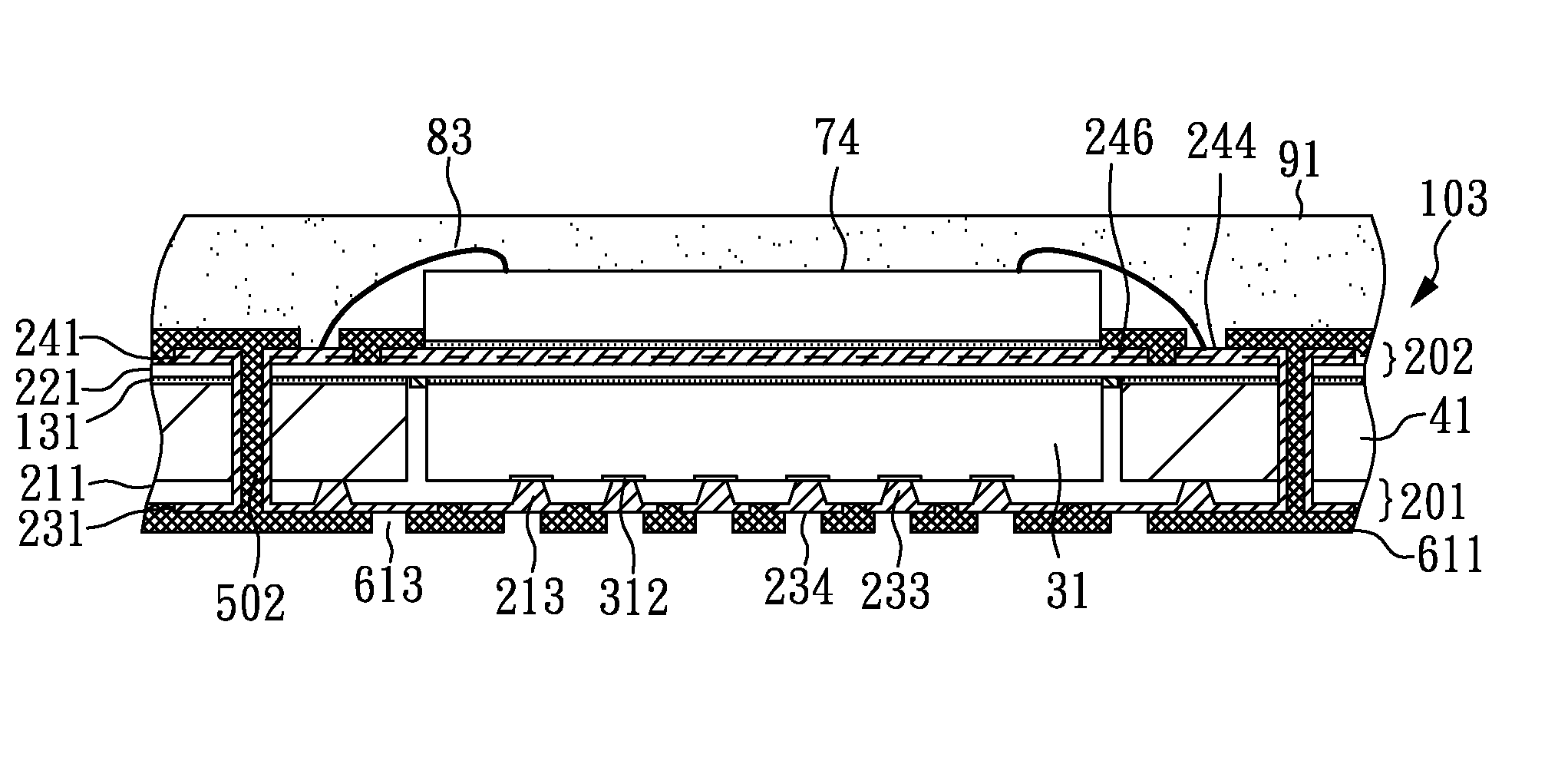
[0067]FIGS. 10 and 10A are cross-sectional and top views, respectively, of another interconnect substrate 102 with placement guide 115 in close proximity to the outer peripheral edges of stiffener 41 and second conductive vias 243 in direct contact with inactive surface 313 of semiconductor device 31 and stiffener 41 in accordance with another embodiment of the present invention.

[0068]In this embodiment, interconnect substrate 102 is manufactured in a manner similar to that illustrated in Embodiment 1, except that placement guide 115 is simultaneously formed during stopper 113 formation by removing selected portions of metal layer 11 to accurately confine the placement location of stiffener 41 and second conductive vias 243 are formed in direct contact with inactive surface 313 of semiconductor device 31 and stiffener 41. Herein, first build-up circuitry 201 includes first insulating layer 211, first conductive traces 231, third insulating layer 251 and third conductiv...

embodiment 3

[Embodiment 3]

[0070]FIGS. 11-16 are cross-section views showing a method of making yet another interconnect substrate with the stopper around the inactive surface of the semiconductor device in accordance with yet another embodiment of the present invention.

[0071]For purposes of brevity, any description in Embodiment 1 is incorporated herein insofar as the same is applicable, and the same description need not be repeated.

[0072]FIG. 11 is a cross-sectional view of the structure which is manufactured by the same steps shown in FIGS. 1-4, except that semiconductor device 31 is mounted on dielectric layer 21 with its inactive surface 313 facing dielectric layer 21.

[0073]FIG. 12 is a cross-sectional view of the structure with first insulating layer 211 formed on active surface 311 of semiconductor device 31 and stiffener 41 in the upward direction. First insulating layer 211 covers semiconductor device 31, stiffener 41 and stopper 113 in the upward direction, and extends into the gap bet...


PUM


Abstract

The present invention relates to an interconnect substrate with an embedded device, a built-in stopper and dual build-up circuitries and a method of making the same. In accordance with one preferred embodiment of the present invention, the method includes: forming a stopper on a dielectric layer; mounting a semiconductor device on the dielectric layer using the stopper as a placement guide for the semiconductor device; attaching a stiffener to the dielectric layer; forming a first build-up circuitry and a second build-up circuitry that cover the semiconductor device, the stopper and the stiffener at both sides; and providing a plated through-hole that provides an electrical connection between the first and second build-up circuitries. Accordingly, the stopper can accurately confine the placement location of the semiconductor device and avoid the electrical connection failure between the semiconductor device and the build-up circuitry.

Description

CROSS REFERENCE TO RELATED APPLICATION[0001]This application claims the benefit of filing date of U.S. Provisional Application Ser. No. 61 / 682,801, entitled “Structure and Manufacture of Semiconductor Assembly and 3D Stacking thereof” filed Aug. 14, 2012 under 35 USC §119(e)(1).BACKGROUND OF THE INVENTION[0002]1. Field of the Invention[0003]The present invention relates to an interconnect substrate for a semiconductor assembly and a method of making the same, and more particularly to an interconnect substrate with embedded semiconductor device and built-in stopper and a method of making the same.[0004]2. Description of Related Art[0005]As market trend demands for thinner, smarter and cheaper portable electronics, semiconductor devices for use in these equipments are required to further shrink their size and improve electrical performances at lower cost. Among all the efforts, embedding or built-in semiconductor chip in printed wiring board to form a module assembly is considered the...

Claims


Application Information

Patent Timeline
Patent Type & Authority Patents(United States)
IPC IPC(8): H01L21/58H01L23/498H01L23/00H01L23/485
CPCH01L21/58H01L23/485H01L23/49822H01L23/49827H01L23/562H01L24/13H01L24/16H01L2224/0401H01L2224/04105H01L2224/131H01L2224/16145H01L2224/16227H01L2924/15172H01L2924/171Y10T428/24917H01L2924/014H01L2224/16225H01L2924/12042H01L2924/00
Inventor LIN, CHARLES W. C.WANG, CHIA-CHUNG
Owner BRIDGE SEMICON
Why Eureka
Try Eureka