
Touch panel

a technology of touch panel and electrode layer, applied in the field of touch panel, can solve problems such as circuit breakage in the electrode layer, and achieve the effect of reducing the height difference between the visual masking layer and the display area covered by the electrode layer and improving the yield rate of the touch panel

Active Publication Date: 2015-09-15
ACER INC
View PDF18 Cites 0 Cited by
  • Summary
  • Abstract
  • Description
  • Claims
  • Application Information

AI Technical Summary

Benefits of technology

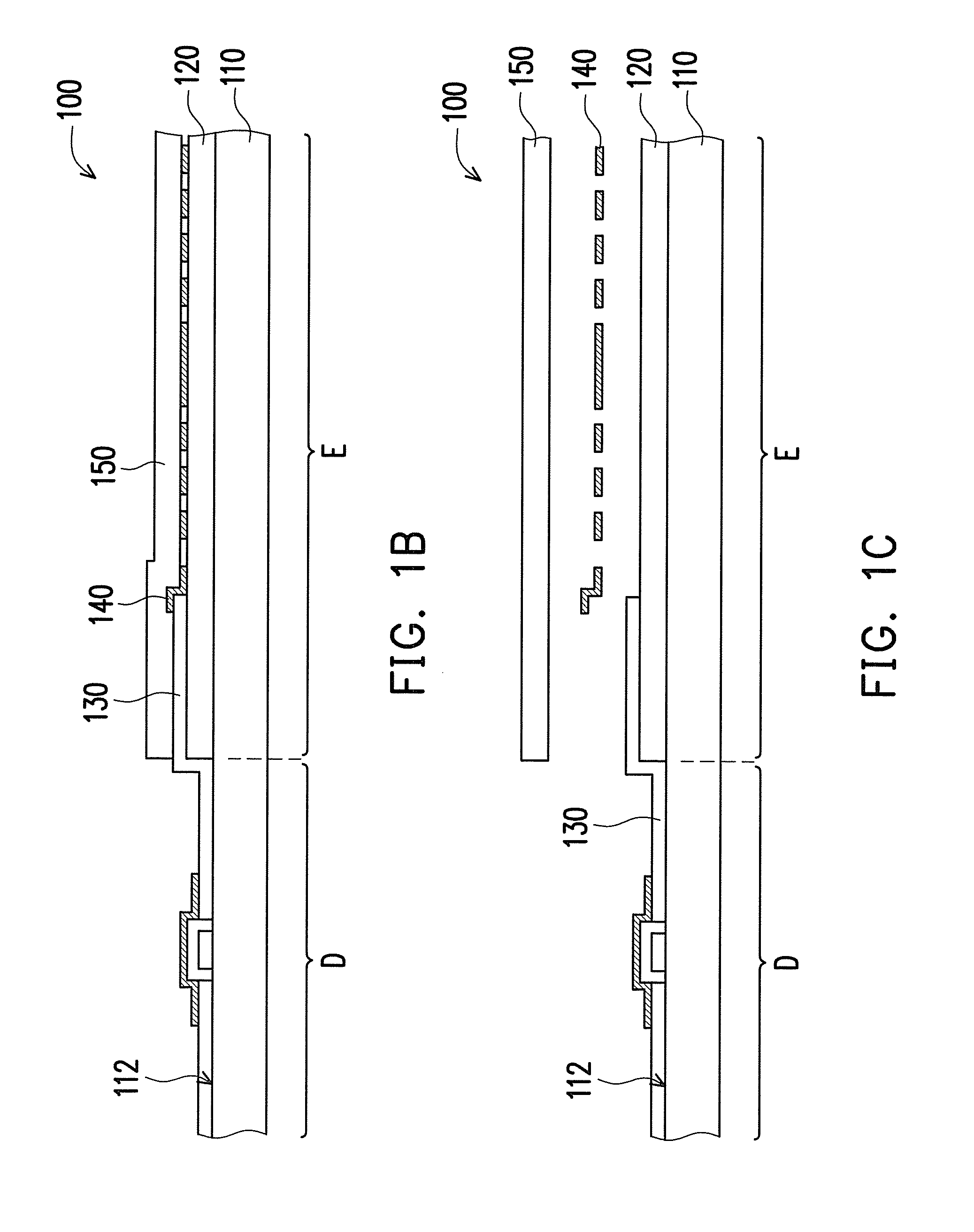
The present invention improves the yield rate of a touch panel by reducing the height difference between a visual masking layer and a display area covered by an electrode layer. This is achieved by using multiple layers for the visual masking layer, where the first layer is placed at the edge area and the second layer is covering the electrode layer. This results in a thicker visual masking layer that maintains the appearance of the touch panel, while also reducing the height difference between the display area and the edge area that could cause circuit breakage.

Problems solved by technology

When an electrode layer is disposed on the surface of the visual masking layer and the surface of the display area, the height difference between the visual masking layer and the display area may cause circuit breakage in the electrode layer.

Method used


Image

  • Touch panel
  • Touch panel
  • Touch panel

Examples


Embodiment Construction

[0027]Reference will now be made in detail to the present preferred embodiments of the invention, examples of which are illustrated in the accompanying drawings. Wherever possible, the same reference numbers are used in the drawings and the description to refer to the same or like parts.

[0028]FIG. 1A is a diagram of a touch panel according to an embodiment of the present invention. FIG. 1B is a cross-sectional view of the touch panel in FIG. 1A along line I-I. FIG. 1C is an exploded view of the touch panel in FIG. 1B. Referring to FIGS. 1A-1C, the touch panel 100 in the present embodiment provides a touch signal. The touch panel 100 includes a substrate 110, a first visual masking layer 120, an electrode layer 130, a metal material layer 140, and a second visual masking layer 150. The substrate 110 has a surface 112. The first visual masking layer 120 is disposed on at least one edge area E of the surface 112.

[0029]After the first visual masking layer 120 is disposed, the electrode ...


PUM


Abstract

A touch panel providing a touch signal is disclosed. The touch panel includes a substrate, a first visual masking layer, an electrode layer, a metal material layer, and a second visual masking layer. The substrate has a surface. The first visual masking layer is disposed on at least one edge area of the surface. A part of the electrode layer is disposed at a display area on the surface adjacent to the edge area, and another part of the electrode layer covers at least a portion of the first visual masking layer. The metal material layer is disposed at the edge area and electrically connected with the electrode layer. The second visual masking layer is disposed at the edge area and stacked on the first visual masking layer. The said another part of the electrode layer is sandwiched between the first visual masking layer and the second visual masking layer.

Description

CROSS-REFERENCE TO RELATED APPLICATION[0001]This application claims the priority benefit of Taiwan application serial no. 102105325, filed on Feb. 8, 2013. The entirety of the above-mentioned patent application is hereby incorporated by reference herein and made a part of this specification.BACKGROUND OF THE INVENTION[0002]1. Field of the Invention[0003]The present invention generally relates to a touch panel, and more particularly, to a touch panel with a visual masking layer.[0004]2. Description of Related Art[0005]In recent years, electronic devices, such as notebooks (NB), tablet PCs, and smart phones, have been widely used in our daily life along with the development of technologies. Some of aforementioned electronic devices are designed very small-sized and light-weighted therefore can be conveniently operated and carried around. Different types of electronic devices with diversified functionalities have been developed, and user-friendliness and practicality of these electroni...

Claims


Application Information

Patent Timeline
Patent Type & Authority Patents(United States)
IPC IPC(8): G06F3/041G06F3/044
CPCG06F3/0412G06F3/044G06F3/0443G06F3/0446
Inventor KUO, JIN-TING
Owner ACER INC
Learn More