Solid-state imaging apparatus and camera
a technology of solid-state imaging and imaging apparatus, which is applied in the field of solid-state imaging apparatus and camera, can solve problems such as reducing dynamic range, and achieve the effect of maintaining dynamic range and improving charge transfer efficiency
- Summary
- Abstract
- Description
- Claims
- Application Information
AI Technical Summary
Benefits of technology
Problems solved by technology
Method used
Image
Examples
first embodiment
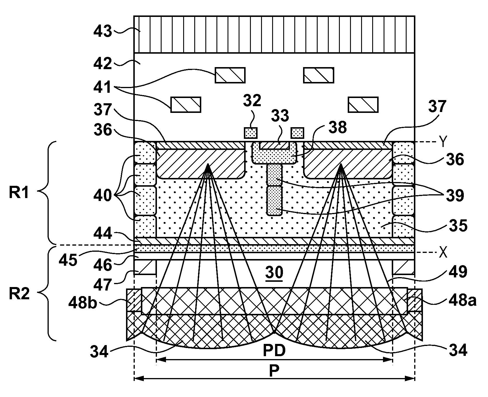
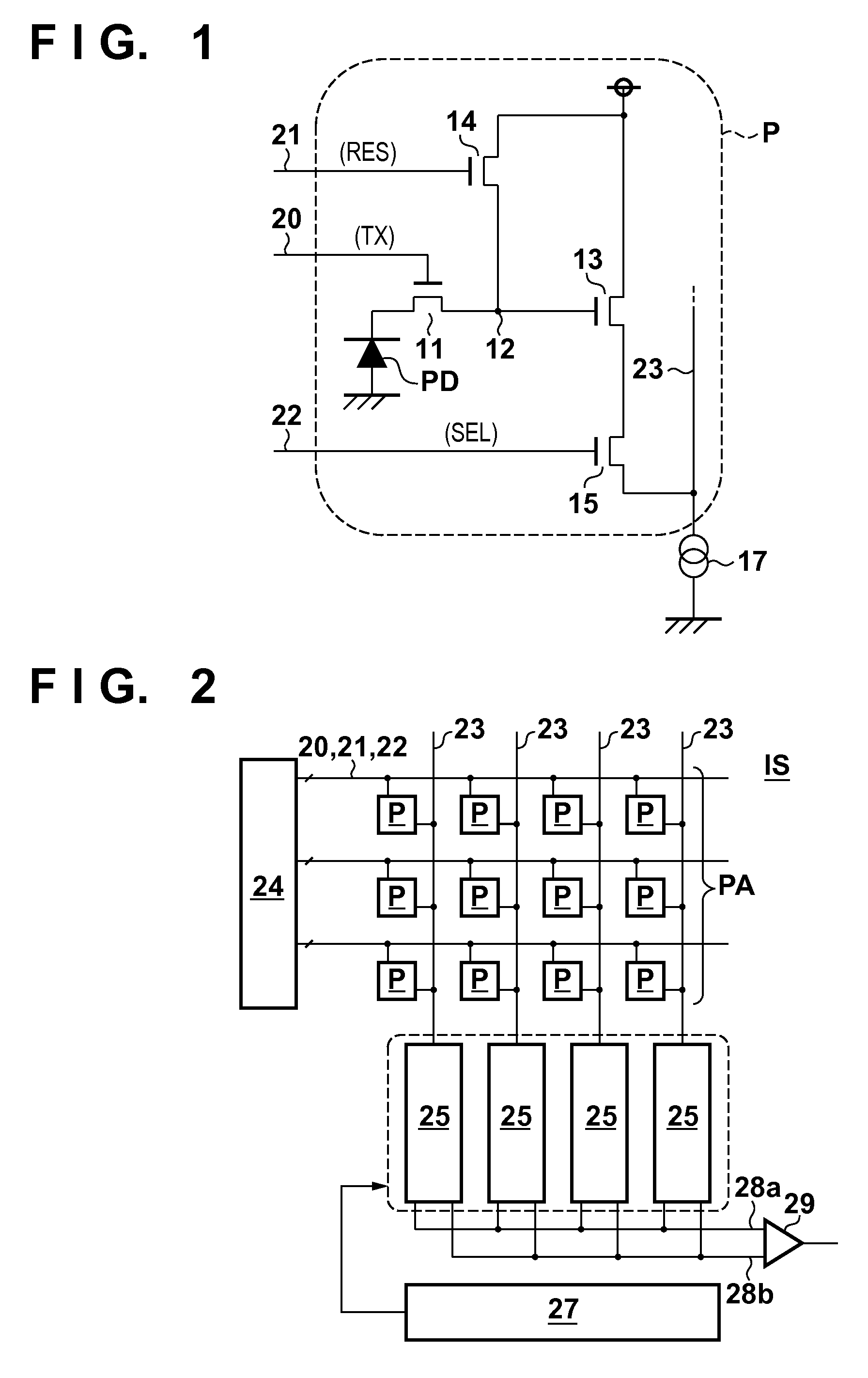
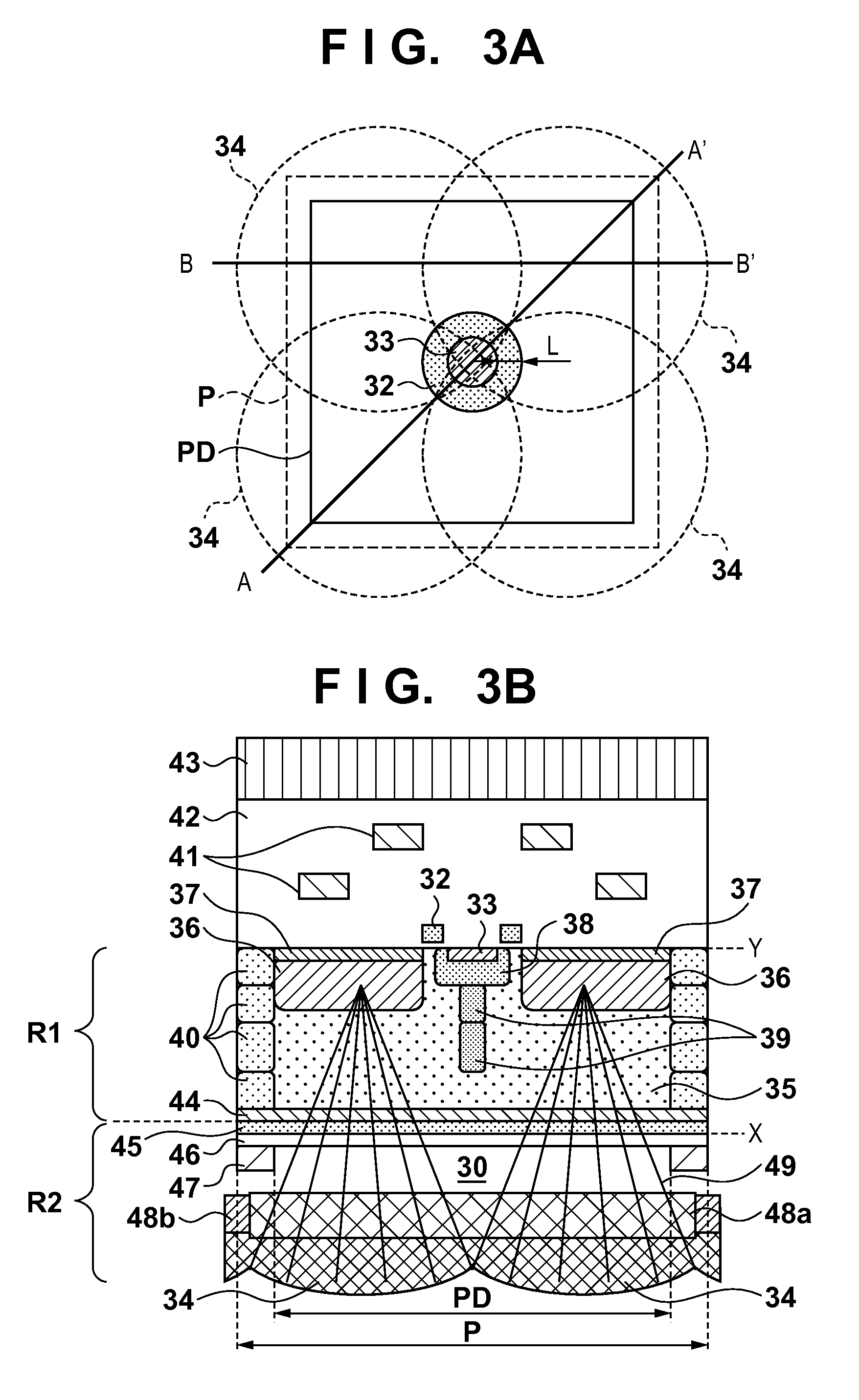
[0025]A solid-state imaging apparatus IS1 according to the first embodiment will be described with reference to FIGS. 3A to 5. FIGS. 3A to 3D schematically show an example of the arrangement of a unit pixel P in the solid-state imaging apparatus IS1. FIG. 3A is a plan view of the pixel P. FIG. 3B is a sectional structural view taken along a cut line A-A′ in FIG. 3A, and FIG. 3C is a sectional structural view taken along a cut line B-B′. In addition, FIG. 3D shows an example of the arrangement of an optical system arranged in correspondence with the pixel P.
[0026]The solid-state imaging apparatus IS1 can include a semiconductor portion R1 which has an X face (first face) and Y face (second face) opposing each other, and an optical system R2 which is arranged on the X face side of the semiconductor portion R1. The X face side is a face side on which light to the solid-state imaging apparatus IS1 enters. Therefore, the solid-state imaging apparatus IS1 is of a back-side illumination ty...
second embodiment
[0046]An solid-state imaging apparatus IS2 according the second embodiment will be described with reference to FIG. 6. FIG. 6 shows a sectional structural view of a unit pixel P in the solid-state imaging apparatus IS2 as in FIG. 3B. The arrangement in which the negative bias is applied to the gate electrode 32 while setting the transfer transistor 11 in a non-conductive state, and the hole pinning state is set near the surface of the semiconductor portion R1 under the gate electrode 32 is exemplified in the first embodiment. However, as in the second embodiment, the arrangement in which a p-type well 38 is electrically connected to a p-type semiconductor region 44 provided on an X face side in a semiconductor portion R1 may be employed.
[0047]The p-type well 38 and p-type semiconductor region 44 can be connected to each other by providing a p-type semiconductor region 39 of the same conductivity type from the X face side to a Y face side. In this structure, a potential of the p-type...
third embodiment
[0048]An solid-state imaging apparatus IS3 according the third embodiment will be described with reference to FIG. 7. FIG. 7 shows a sectional structural view of a unit pixel P in the solid-state imaging apparatus IS3 as in FIG. 3B. The third embodiment is different from the second embodiment in that a light-shielding member 60 is provided between a semiconductor portion R1 and an optical system R2 so as to make a light intensity inside an n-type semiconductor region 33 low. The light-shielding member 60 can be arranged so that at least a part of orthogonal projection for the semiconductor portion overlaps the n-type semiconductor region 33. In other words, the light-shielding member 60 can be arranged on a normal of the Y face passing through the n-type semiconductor region 33. According to the third embodiment, in the semiconductor portion R1, a light intensity distribution can be formed so as to make the light intensity higher outside of the n-type semiconductor region 33 than in...
PUM
 Abstract
Description
Claims
Application Information
 - R&D
- Intellectual Property
- Life Sciences
- Materials
- Tech Scout
- Unparalleled Data Quality
- Higher Quality Content
- 60% Fewer Hallucinations
Browse by: Latest US Patents, China's latest patents, Technical Efficacy Thesaurus, Application Domain, Technology Topic, Popular Technical Reports.
© 2025 PatSnap. All rights reserved.Legal|Privacy policy|Modern Slavery Act Transparency Statement|Sitemap|About US| Contact US: help@patsnap.com


